


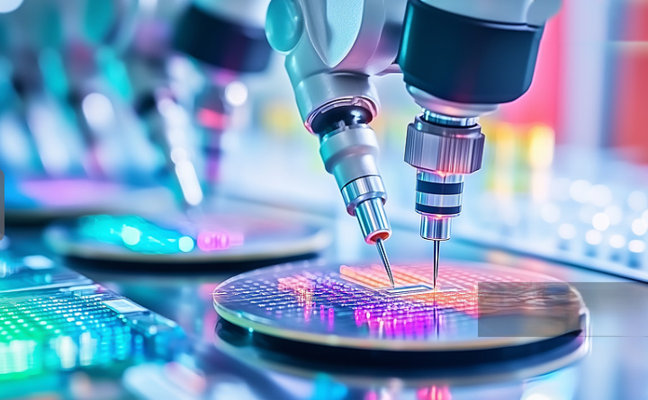
InIn the precision-driven world of semiconductor manufacturing, every link in the production chain is intricately connected, with the uniformity of gas distribution playing a pivotal role in determining the quality of wafer fabrication. The key gas distribution device developed and produced by AMTD acts as the "conductor" of gas flow within the semiconductor manufacturing process, precisely and orderly regulating the direction and distribution of gases—its importance cannot be overstated.
This gas distribution device boasts an exquisitely designed structure. It is meticulously crafted using high-precision machining equipment. AMTD has proactively planned and introduced cutting-edge processing machinery, which, akin to skilled artisans, ensures the highly consistent pore diameters across the device. Each pore serves as a precise conduit, allowing gases to pass through uniformly and spread evenly across the wafer surface. This uniformity is crucial for film formation, as only with evenly distributed gases can a uniform and consistent film layer be achieved, thereby laying a solid foundation for subsequent chip manufacturing. Should gas distribution be uneven, the film layer would exhibit variations in thickness, severely impacting chip performance and yield rates.
Semiconductor manufacturing demands an almost obsessive level of cleanliness, as even the slightest impurity can cause irreversible damage to wafers. Consequently, the gas distribution device produced by AMTD undergoes rigorous cleaning processes throughout its manufacturing journey. From initial raw material cleaning to intermediate cleaning at various processing stages, and finally to finished product purification, every step is meticulously controlled to eliminate any trace of contamination. Advanced cleaning techniques and agents are employed to remove oil stains, dust, metal particles, and other pollutants from the device's surface, ensuring its cleanliness meets the stringent standards of semiconductor manufacturing.
In addition to high precision and cleanliness, the device's surface undergoes multiple treatment processes. AMTD achieves a smooth and even surface through physical polishing, reducing resistance during gas flow; sandblasting increases surface roughness, enhancing coating adhesion; anodizing forms a dense oxide film, effectively improving the device's corrosion resistance; and nickel brushing enhances surface wear resistance, extending the device's service life. These processes work in synergy, enabling the device to operate stably in the complex semiconductor manufacturing environment and providing reliable gas distribution for wafer fabrication.
As semiconductor manufacturing continues to evolve, the demands placed on gas distribution devices are escalating. AMTD's key device will persistently undergo technological innovation and optimization upgrades to meet the needs of more advanced manufacturing processes and higher production requirements. It will continue to play a pivotal role as the "conductor" in the semiconductor manufacturing process, steering the semiconductor industry towards higher precision and quality.


