


I. Introduction to Positions in Semiconductor Fab
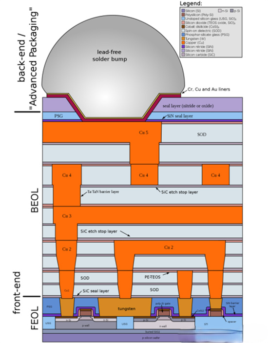
The following is a schematic diagram of the internal structure of an integrated circuit:
The 3D schematic of a chip structure is shown below:
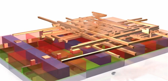
Essentially, the internal physical structure of a chip is a stack of multiple patterned layers with ordered interconnections between them.
In terms of materials, each layer is composed of semiconductor materials, conductor materials, or insulator materials.
Based on the sequence of process steps, they can be broadly divided into the Front-End-Of-Line (FEOL) and Back-End-Of-Line (BEOL).
Simply put, the FEOL is primarily responsible for forming CMOS transistor structures, while the BEOL handles metal wiring.
Achieving these structures mainly involves the coordinated efforts of several major process modules: photolithography, etching, thin-film deposition, Chemical Mechanical Polishing (CMP), and Implant.
These processes involve interacting with Modules in the Fab, where a module refers to the department responsible for each specific process.
II. Introduction to Main Processing Steps in the Fab
1. FUR (Furnace) - Furnace Operations
As a Process Integration Engineer (PIE), the main tasks requiring interaction with FUR involve oxide growth and annealing.
Heating is energy-intensive and costly, so the number of ANNL (annealing) sites is strictly controlled within the factory, resulting in low autonomy for Process Engineers (PEs) in this department (personally, I also feel this reduces the department's value). Additionally, any trial applications for FUR Recipe (RCP) must be approved through meetings, unless a new process flow is being established. This differs from other departments where communication with PEs suffices. PIEs only need to know the available FUR conditions in the factory and generally do not create new conditions for individual products.
All furnace processes require pollution control, and a pre-cleaning process is mandatory before entry to prevent contamination. Generally, exposed poly (polysilicon) indicates a contamination risk, while full oxide coverage suggests no contamination.
(a) Oxide Growth - Dry Oxidation
This typically involves the reaction Si + O2 = SiO2.
This method consumes Si from the wafer's epitaxial layer, generating SiO2 at a ratio of 45:100. The growth rate decreases as the thickness of SiO2 increases because oxygen has more difficulty contacting the silicon. Dry oxidation produces the highest quality oxide with the fewest internal defects but has the slowest growth rate. Process temperatures range from 900-1200°C, and temperatures below 700°C are unsuitable.
It is typically used for growing oxides less than 1000 Å (1 Å = 10^-10 m = 0.1 nm; the correct symbol for Å is a circle above the letter A, pronounced "angstrom"), such as Gate Oxidation, a critical process that determines the threshold voltage (Vth) of MOSFETs.
(b) Oxide Growth - Wet Oxidation
Hydrogen and oxygen are introduced into the chamber in a specific ratio to generate water (H2O). The reaction 2H2O + Si = SiO2 + 2H2 then produces SiO2. Hydrogen is not consumed in this process, and continuous gas exchange in the furnace prevents explosions. The hydrogen-to-oxygen ratio must be kept below 2:1, typically at 1.8:1. This method grows SiO2 more rapidly and consumes Si at a ratio of 0.45. It can theoretically be used for growing SiO2 layers from 0 to 20,000 Å thick, although applications rarely exceed 10,000 Å.
Wet oxidation is chosen to balance quality and cost. For growing thick oxides (several thousand angstroms), dry oxidation is impractical due to its slow rate. While Chemical Vapor Deposition (CVD) can also be used, it often results in incomplete deposition at the bottom and corners, low oxide density, and poor electrical properties. Wet oxidation offers a reliable compromise.
(c) Annealing
When IMP injects ions (such as phosphorus (P), arsenic (As), boron (B), or gallium (Ga)) into silicon, the atomic lattice is damaged, and the injected ions are not in their proper lattice sites but in interstitial positions. Annealing is required to repair lattice defects and activate the injected ions, allowing them to occupy lattice sites. This is generally a fixed process, following customer-specified conditions. The annealing process determines the depth of ion penetration, i.e., the depth of P-type and N-type regions.
PS: This process is somewhat similar to dry oxidation, as it also produces a thin oxide layer (5-20 nm). Pure oxide can block the diffusion of phosphorus, thus altering the contamination level of the wafer. When engineering wafers skip the IMP step, this must be taken into account.
(d) Rapid Thermal Annealing (RTA)
RTA involves treating the wafer at extremely high temperatures for a very short duration (e.g., 30 seconds). Due to the brief treatment time, ions can be activated while minimizing diffusion. This is valuable for fabricating ultra-shallow junctions and is expected to see increased application.
2. IMP (Implant) - Ion Implantation
Ion implantation is a process that uses a high-energy machine to create a large electromagnetic field, from which ionized ions are ejected (since only charged particles can be accelerated) and injected into the epitaxial layer of the wafer. This is a purely physical process involving the injection of ions. After implantation, electroneutralization is performed to ensure the wafer is electrically neutral.
The purpose of this process is to dope specific regions of the wafer with specific concentrations of ions to form P-type and N-type regions, which then constitute PN junctions and structures like NPN transistors.
The PIE's interaction with IMP primarily involves creating new Recipes (RCPs). The PIE acts as a bridge between the customer and IMP, using simulation results to determine the required IMP dose, energy, angle, and ion species. They then check if a corresponding RCP exists and request its use via email or apply for a new RCP if none exists. The PIE also consults with IMP to ensure machine availability (as IMP and FUR machines often have cargo restrictions, and unavailability can lead to late-night calls or even overtime). The workload in this department is unclear, but the challenges likely lie with the equipment manufacturers. Despite this, the department is very busy, as each product condition is unique, and RCPs are constantly being created (possibly due to high staff turnover). PIEs typically need to submit requests several days in advance, as the department is not easy to communicate with.
IMP involves four parameters: dose, energy, angle, and ion species. The dose refers to the number of ions to be injected per unit area onto the wafer surface, determining the doping concentration and influencing the threshold voltage (Vth). Energy, acquired by ions accelerated in an electric field, determines the injection depth. Changing the energy usually requires adjusting the channel depth, which also affects Vth. The classic injection angle is 22°, avoiding direct injection into deep lattice gaps, unlike a 0° angle. While much of this is determined during simulation, there is still much to learn.
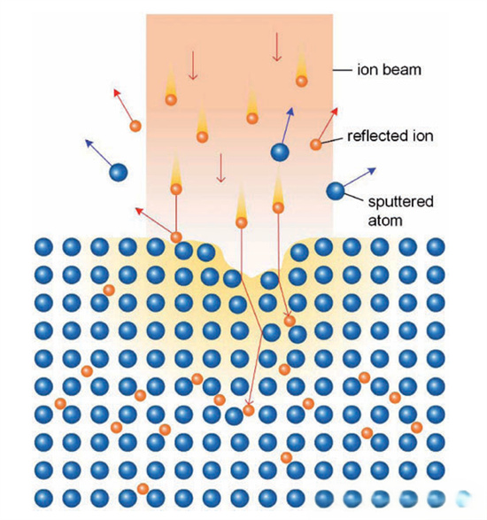
Ion implantation is typically performed uniformly (blanket implantation). Areas not requiring implantation are covered with photoresist (PR) or thick thermal oxide to block the ions. IMP is closely linked with the WET (wet etching) department and has some association with PH (possibly referring to photolithography).
3. WET (Wet Etch) - Wet Etching
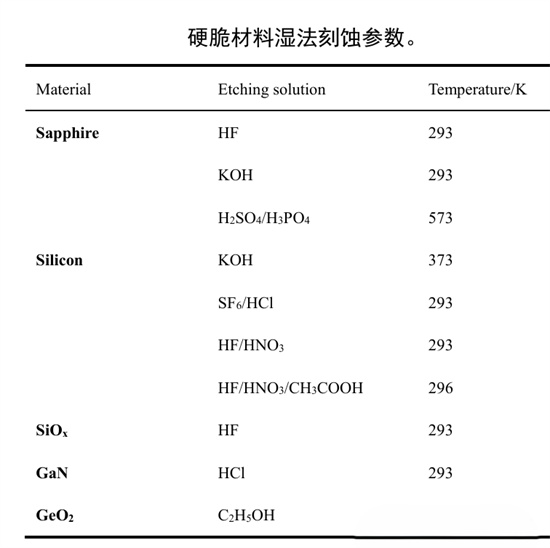
Wet etching is an isotropic etching process that uses chemical solutions. In this process, the wafer is immersed in a liquid, and all surfaces exposed to the liquid are etched. In contrast, dry etching is like exposing the wafer to sunlight, where only the illuminated areas are etched.
Wet etching is commonly used for removing SiO2 and Si, as well as other materials like SiN. A typical etchant is a mixture of hydrofluoric acid and ammonium fluoride in a ratio of 1:several dozen, although dozens of other chemical solutions are available for various processes, with training provided upon joining the company. In 12-inch fabs, direct contact with these chemicals is rare, eliminating safety concerns. However, in 8-inch and 6-inch fabs, manual wafer etching processes may require direct contact with chemicals, so it is essential to inquire about this before joining.
Isotropic etching is a characteristic of WET, making it difficult to create specific patterns using photoresist alone, which is a limitation compared to dry etching. Additionally, care must be taken to prevent the etchant from penetrating beneath the photoresist and causing undercutting, which can occur during ion implantation. However, isotropic etching also has advantages, such as the ability to perfectly remove oxide from sidewalls. In contrast, dry etching often creates angled sidewalls, leaving residues in deep recesses that require additional processing to remove.
When confirming Photoresist Strip (PRS), PIEs typically use existing conditions to scrap wafers and perform Scanning Electron Microscope (SEM) tests to check if the morphology meets requirements. They then provide before-and-after morphology images to PEs, who can roughly calculate the etching rate (as the morphology changes during etching and the clear ratio varies by product). Based on the etching rate, an RCP is provided to optimize PRS until requirements are met.
WET is commonly used for forming channels in power devices, where depth is a critical parameter. Multiple cross-sectional checks may be required to confirm the process, unlike FUR and IMP, where approval is generally sufficient.
Different oxides, such as thermal oxide, Plasma-Enhanced Tetraethyl Orthosilicate (PETEOS), Ozone Tetraethyl Orthosilicate (OZTEOS), and High-Density Plasma (HDP) oxide, have varying etching rates, depending on the film structure.
Overall, this department seems to have a higher technical content, although most etching sites have been replaced by dry etching. However, wet etching remains essential (and all cleaning sites use wet processes).
III. Introduction to Thin Film Growth Technologies
The Thin Film (TF) department includes three sub-departments: Physical Vapor Deposition (PVD), Chemical Vapor Deposition (CVD), and CMP. Each has significant technical depth, with PVD and CVD involving extensive research into film properties, types, and trench filling.
1. Physical Vapor Deposition (PVD)
PVD is a process where atoms are physically sputtered and deposited layer by layer onto the wafer, resulting in an amorphous material (which can be recrystallized through annealing). The wafer temperature is typically kept below 100°C during deposition, and an ultra-high vacuum environment (<10^-10 mTorr) ensures high film quality.
2. Chemical Vapor Deposition (CVD)
CVD involves introducing mixed gases into a chamber where they react to deposit a thin film on the wafer surface. The gases are stable at room temperature, and the wafer is heated to a high temperature to facilitate the reaction.
There are various types of oxides:
The most common is SiO2, deposited by oxidizing silane (SiH4) with oxygen (O2) or nitrous oxide (N2O).
Doped oxides, such as Phosphosilicate Glass (PSG), Borophosphosilicate Glass (BPSG), and Fluorosilicate Glass (FSG), are used for Interlayer Dielectric (ILD) and Intermetal Dielectric (IMD) layers, crucial for passing reliability tests like High-Temperature Reverse Bias (HTRB), High-Temperature Gate Bias (HTGB), and High-Temperature Humidity Reverse Bias (H3TRB) for 1000 hours at 175°C (required for automotive-grade power chips). Consumer products typically require only 150°C for 500 hours.
Isolation oxides like Ozone Tetraethyl Orthosilicate (O3TEOS), a reaction product of ozone and tetraethyl orthosilicate, can be used to increase device breakdown voltage. For thick oxides, a combination of thermal oxidation and TEOS deposition is common, especially in power devices, and even for gate oxide growth. TEOS offers excellent step coverage, avoiding weak filling at corners.
High Aspect Ratio Process (HARP) deposition is used for trench filling, with a reaction mechanism similar to TEOS but capable of filling ratios exceeding 4:1 or 5:1, commonly used below the 90nm node. To achieve higher filling ratios, HARP may be alternated with etching processes, similar to High-Density Plasma (HDP) CVD.
Silicon nitride (Si3N4) deposition is used for various purposes, such as stress engineering to reduce wafer warping, impurity ion isolation, insulation, and as a CMP stop layer, due to its high dielectric constant and other functions.
These functions are all relevant during process flow development. The excellent step coverage is due to the reaction and nucleation on the wafer surface before film formation, unlike PVD, which deposits material directly in the vacuum.
3. Chemical Mechanical Planarization (CMP)
CMP is used to planarize the wafer surface.
The need for CMP arises because previous processes like CVD, PVD, etching, and furnace operations can leave the wafer surface uneven, with significant height differences within the same film layer.
During CMP, a polishing head applies pressure and rotates while moving across the wafer surface. Abrasive materials are continuously added, and the wafer undergoes both physical and chemical reactions, gradually thinning to a specific thickness.
Chemical reactions are crucial in CMP, preventing reliance solely on mechanical abrasion. This allows the process to stop at a specific stop layer, achieving excellent surface planarization. CMP systems also include monitoring to measure film thickness at multiple points on the wafer in real-time, adjusting the polishing head pressure to ensure uniformity.
When a CMP process needs to be added to a process flow to meet morphological requirements, the PIE collaborates with CMP PEs to develop the process. The PIE selects measurement locations and thickness parameters for the Advanced Process Control (APC) system and provides feedback to CMP for RCP adjustments.
Since measurement locations are often not at the core of power devices, the PIE must perform multiple cross-sectional checks to correlate measurement points with actual thickness and define an acceptable range. After CMP, the wafer surface is relatively flat but may still have variations of 100 nm to several micrometers. CMP is expensive and should be avoided if possible. AMTD provides high-precision Showerhead services for core components, including products like Shower heads, Face plates, Blocker Plates, Top Plates, Shields, Liners, pumping rings, and Edge Rings, widely used in semiconductor and display panel industries, known for their exceptional performance and high market recognition.
Source: Zhihu, Author: Xinghuo Diandeng You Ge Meng (Starfire Lighting a Dream)


