


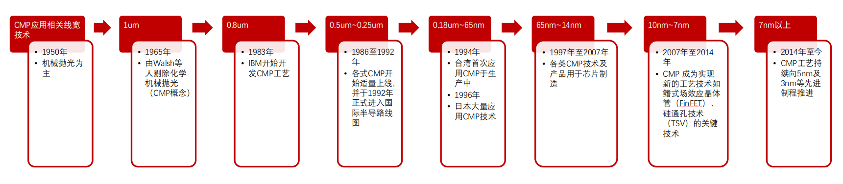
The concept of Chemical Mechanical Polishing (CMP) was first proposed by Walsh et al. in 1965 and has since evolved into an indispensable part of IC (Integrated Circuit) manufacturing processes. As chip fabrication technology has advanced, CMP technology has also evolved through innovations in materials such as aluminum, copper, low-k dielectrics, and cobalt.
Several key milestones have marked the development trajectory of CMP polishing technology:
At the 0.18μm–0.13μm technology nodes, with copper officially replacing aluminum as the mainstream conductive material, CMP became an indispensable process step for copper interconnect technology. As the technology node evolved to 65nm, low-k dielectric materials, introduced to reduce RC delay, gradually replaced traditional SiO₂. However, conventional CMP techniques, due to their higher pressures, often caused collapse or delamination of low-k materials, making them difficult to apply below the 65nm node. Consequently, the development of low-pressure CMP equipment suitable for low-k dielectric materials emerged as a new research direction.
When the technology node advances to the 30–20 nm range, Cu (Copper) interconnection is no longer suitable for interconnection technologies below 20 nm, which forces people to start developing new interconnection materials and technologies. CMP (Chemical Mechanical Polishing) technology applied to cobalt interconnection has become another development direction.
When the integrated circuit node develops to 14 nm, CMP (Chemical Mechanical Polishing) has evolved into a key technology for realizing new process technologies such as Fin Field-Effect Transistor (FinFET) and Through-Silicon Via (TSV). Nowadays, as semiconductor manufacturing processes progress from 14 nm to 7 nm, 5 nm, and even 3 nm nodes, the number of CMP process steps will surge from about a dozen to over 30.
Core Functions of CMP
CMP achieves nanometer-level planarization of the wafer surface through the synergistic effect of chemical corrosion and mechanical polishing. Its core challenges include:
1.Material Selectivity: Precise control of the differential removal rates of different materials (such as copper, dielectric layers, and barrier layers) is required.
2.Global Uniformity: The thickness deviation at any point on a 300 mm wafer must be less than 1 nm.
3.Defect Suppression: Avoiding critical defects such as scratches, corrosion pits, and residual particles.
In the 14 nm era, CMP already needed to address the planarization of interconnection structures with over 10 layers, but the 3 nm node has pushed this complexity to new heights. When the feature size shrinks to 3 nm, it is equivalent to 20 silicon atoms arranged side by side. At this point:
1、 Surface roughness must be controlled below 0.1 nm RMS (equivalent to the fluctuation of a single atom).
2、The aspect ratio of metal interconnections exceeds 5:1, significantly increasing the difficulty of filling and polishing.
3、Interface effects dominate material behavior, rendering traditional bulk material models ineffective.
These changes force the CMP process to shift from "coarse tuning" to "micro-operation," with step refinement becoming an inevitable choice and an increase in the number of steps an inevitable trend.
Impact of Technological Advancements on CMP
n FinFET structures, the key steps of CMP encompass: Fin Formation: Achieving uniform fin height (±0.5 nm) through STI CMP.
Dummy Gate Polishing: Ensuring the flatness for subsequent high-k dielectric/metal gate deposition.
Thickness Control: Polishing of 200 nm dielectric layers requires ±2 nm uniformity.
Multi-Step Polishing: First, complete 90% of the removal using a soft pad and low pressure, followed by finishing with a hard pad and precise control.
Novel Polishing Slurries: Introduce benzotriazole (BTA) derivatives as corrosion inhibitors.
Global Planarization of Copper Interconnects: Layer-by-layer polishing of 10-12 metal stacks.
At this point, the number of CMP steps is approximately 12-15, with an increase of about 10-15% for each node.
Gate-All-Around Field-Effect Transistors (GAAFETs) employ a vertically stacked nanosheet structure, leading to a reconfiguration of the CMP process:
Nanosheet Release Process: This requires selective removal of SiGe in a SiGe/Si stack, involving: Initial SiGe layer CMP (to control the etching stop surface).Multiple local planarizations (to address stress deformation during the release process)
Multi-Layer Gate Integration: Each nanosheet requires independent gate encapsulation, resulting in: Stepwise polishing of gate metals (such as TiN, WF₆) and precise thickness control of interface passivation layers (such as AlOₓ).
3D Contact Structures: Self-Aligned Contacts (SAC) necessitate: Alternating polishing of dielectric/metal layers (to prevent short circuits) and sidewall protection of contact holes (introducing novel barrier layer CMP).
The changes in transistor structure alone result in an increase of 5-8 CMP steps.
When interconnect linewidths shrink below 10 nm, traditional copper dual damascene processes face fundamental challenges:
Electromigration Failure: At the 3 nm node, current densities exceed 10⁷ A/cm², drastically reducing copper line lifetimes.
Aspect Ratio Disaster: An aspect ratio of 20:1 causes void formation during copper filling. At this point, copper interconnects have to transition to cobalt (Co) and ruthenium (Ru) interconnects, simultaneously bringing about CMP process transformations:
Cobalt Polishing: Co forms easily removable Co²⁺ ions at pH < 4, but issues such as selectivity with Ta/TaN barrier layers and surface passivation control must be addressed.
Ruthenium Direct Deposition Polishing: Ru does not require a barrier layer but introduces new challenges: Reconfiguration of the chemical-mechanical synergy mechanism, where Ru forms polishable RuOₓ in the presence of oxidizing agents. Differences in removal rates dependent on crystal plane orientation necessitate the development of isotropic polishing slurries.
To achieve RC delay control, the 3 nm node adopts ultra-low-k dielectrics with k < 2.4, whose CMP pain points include:
Mechanical Strength Collapse: Porosity > 40% leads to easy collapse during polishing.
Chemical Sensitivity: Traditional SiO₂ polishing slurries can corrode organosilicate glasses.
In-Situ Monitoring: Employ acoustic emission sensors for real-time detection of dielectric layer breakthrough.
This increases the number of dielectric layer CMP steps from 1 to 3.
From 14 nm to 3 nm, the doubling of CMP process steps is an inevitable outcome of semiconductor technology evolution.
Changes in transistor structures, the increase in interconnect layers, the introduction of new materials, and the application of 3D integration technologies all make CMP play an even more critical role in advanced manufacturing processes.
Although the increase in steps poses challenges in terms of cost, yield, and integration complexity, through technological innovation and process optimization, CMP will continue to support the semiconductor industry's progression toward smaller nodes.
In the future, as smaller process nodes become more widespread, the complexity of CMP processes may further increase, becoming one of the core technologies driving the continuation of Moore's Law.
AMTD provides high-precision Showerhead services for core components, with products mainly including Showerhead, Faceplate, Blocker Plate, Top Plate, Shield, Liner, Pumping Ring, Edge Ring, and other core components of semiconductor equipment. These products are widely used in the semiconductor, display panel, and other fields, with excellent performance and high market recognition.


