


As an efficient surface treatment technology, the sandblasting process demonstrates its unique application value in the treatment of semiconductor components. This process utilizes high-speed ejected sand particles to impact the surface of workpieces, creating a certain degree of roughness to improve some of the mechanical properties and surface conditions of the components.

In semiconductor manufacturing, the sandblasting process is commonly used to treat key components such as wafer carrier rings and metal lead frames. Through sandblasting treatment, the surface of workpieces can be effectively roughened, increasing the surface roughness. This, in turn, enhances the adhesion between the workpiece and subsequently deposited film layers or welding materials, ensuring a firm connection. Meanwhile, sandblasting can remove defects such as oil stains, oxide scales, and burrs.
The presence of these defects can lead to issues like poor welding and film layer blistering, affecting the reliable manufacturing of semiconductor devices. Sandblasting treatment also improves the wear resistance and corrosion resistance of components and enhances their appearance quality, providing strong support for the long-term stable operation of semiconductor devices.
The selection of sandblasting media is crucial for the treatment effect. Mineral sand abrasives, such as aluminum oxide and silicon carbide, are characterized by high hardness and good wear resistance. They are suitable for treating high-hardness metal materials, such as stainless steel lead frames, effectively removing surface oxide layers and burrs. On the other hand, artificial sand abrasives, such as glass sand and stainless steel sand, offer the advantages of uniform particle size and smooth surface.
They are applicable in scenarios with high surface quality requirements, such as the treatment of precision wafer carrier rings, preventing excessive surface damage. In addition, the introduction of wet sandblasting technology, which mixes liquid into the sand particles, effectively addresses the dust pollution problem caused by dry sandblasting, improving the cleanliness of the working environment and meeting the strict cleanliness requirements of semiconductor manufacturing.
With the development of semiconductor technology, micro-sandblasting technology has gradually emerged. For micro-packaged components, such as QFN (Quad Flat No-leads) packages, by adjusting the particle size of the sandblasting media, ejection pressure, and angle, precise roughening of the package surface can be achieved. This not only improves welding reliability but also avoids excessive damage that could lead to a decline in component performance.
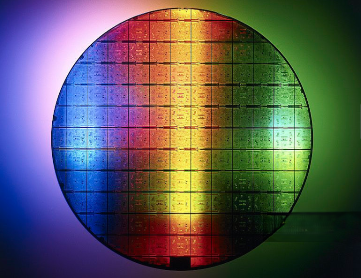
AMTD provides high-precision Showerhead (spray head/gas distribution plate/gas diffuser) services for core components. Its products mainly include semiconductor equipment core parts such as Showerhead, Face plate, Blocker Plate, Top Plate, Shield, Liner, pumping ring, and Edge Ring. These products are widely applied in fields such as semiconductors and display panels, boasting excellent performance and high market recognition.
Content sources: Advanced Packaging Technology, Introduction to Surface Treatment Processes
上一篇:The Core Position of Surface Treatment Processes in Semiconductor Manufacturing
下一篇:Efficient Ultrasonic Cleaning for Semiconductor Particle Removal


