


In the highly sophisticated field of semiconductor manufacturing, surface treatment processes occupy a pivotal and core position. The manufacturing precision requirements for semiconductor devices reach the nanometer level. Any minor surface defects, such as particles, scratches, oxide layers, etc., can significantly impact device performance, including a decline in electrical performance, an increase in leakage current, and a reduction in reliability. Therefore, surface treatment processes have become a crucial link in ensuring the quality and reliability of semiconductor devices.

Surface treatment modifies the material surface through physical, chemical, or mechanical methods, aiming to remove organic substances, inorganic impurities, and oxide films from the surface, thereby improving the performance of the material surface. In semiconductor manufacturing, this process not only relates to the electrical performance of the devices but also directly affects their stability and lifespan.
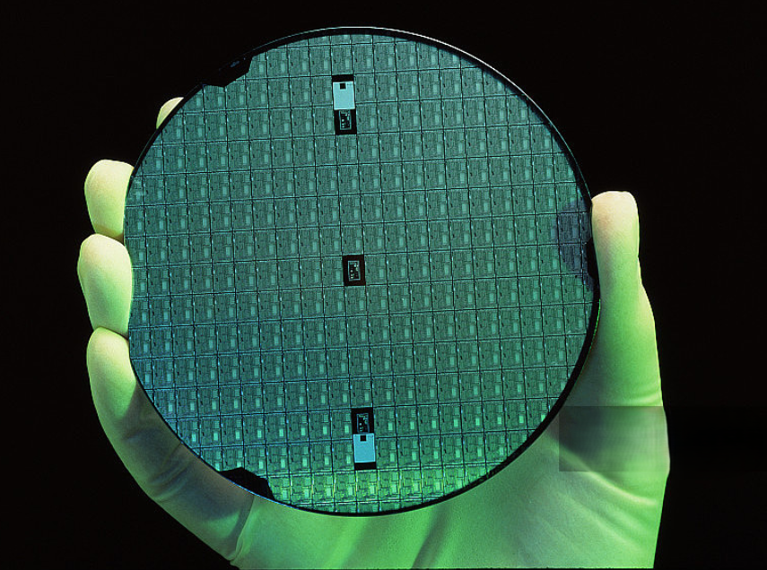
For instance, during the wafer manufacturing process, precise cleaning processes can effectively remove particles and contaminants from the wafer surface. If these particles and contaminants are not removed, they can cause defects during subsequent photolithography, etching, and other processes, such as line breakage and short circuits, which seriously affect device performance.
Physical polishing, as an important means of surface treatment, is widely used for the planarization of semiconductor wafers. Through mechanical grinding, tools such as sandpaper, pneumatic grinders, and chemical-mechanical polishing (CMP) equipment are employed to remove burrs, scratches, and uneven portions on the wafer surface, enhancing the luster and surface quality of the wafer.
The CMP technology combines the advantages of chemical corrosion and mechanical grinding. The chemical components in the polishing slurry react with the material on the wafer surface, softening the surface layer, which is then removed by mechanical grinding. This achieves global planarization, providing an extremely flat substrate for subsequent photolithography processes. It ensures the precise transfer of photolithography patterns and is of utmost importance for advanced process nodes of 7nm and below.
In addition, surface treatment processes also include plasma cleaning. This process utilizes active particles (such as ions and free radicals) in the plasma to clean and activate the wafer surface. It can effectively remove organic contaminants, increase surface energy, and enhance the adhesion of film layers in subsequent processes. This process is widely used in the surface treatment of wafers before chip packaging, contributing to improved packaging reliability.
AMTD provides high-precision Showerhead (spray head/gas distribution plate/gas diffuser) services for core components. Its products mainly include semiconductor equipment core parts such as Showerhead, Face plate, Blocker Plate, Top Plate, Shield, Liner, pumping ring, and Edge Ring. These products are widely applied in fields such as semiconductors and display panels, boasting excellent performance and high market recognition.
Content sources: Semiconductor Manufacturing Technology Handbook, Introduction to Surface Treatment Processes
上一篇:A Comprehensive Upgrade from Protection to Functionality
下一篇:The Unique Application of Sandblasting Process in Semiconductor Component Treatment


