


In the semiconductor manufacturing sector, as device dimensions continue to shrink, unprecedented challenges have been posed to thin-film deposition technologies. Atomic Layer Deposition (ALD), a thin-film deposition technique capable of achieving atomic-level precision control, has become an indispensable part of semiconductor fabrication. This article aims to provide an in-depth introduction to the ALD process flow and principles, facilitating an understanding of its crucial role in advanced chip manufacturing.
I. Detailed Explanation of the ALD Process Flow
The ALD process adheres to a strictly sequential procedure, ensuring that only one atomic layer is added per deposition cycle, thereby enabling precise control over film thickness. The fundamental steps are as follows:
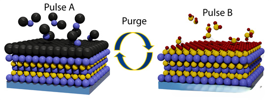
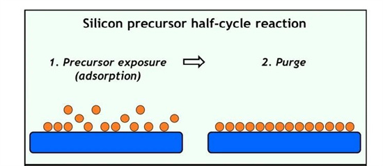
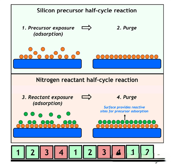
1. Precursor Pulse: The ALD process commences with the introduction of the first precursor into the reaction chamber. This precursor, a gas or vapor containing the chemical elements of the target deposition material, reacts with specific active sites on the wafer surface. Precursor molecules adsorb onto the wafer surface, forming a saturated molecular layer.
2. Inert Gas Purge: Subsequently, an inert gas (such as nitrogen or argon) is introduced to purge the chamber, removing unreacted precursors and by-products. This ensures a clean wafer surface, preparing it for the next reaction step.
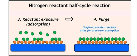
Second Precursor Pulse: After the purge, the second precursor is introduced, reacting chemically with the precursor adsorbed in the first step to generate the desired deposit. This reaction is typically self-limiting, meaning that once all active sites are occupied by the first precursor, no further reaction occurs.
· Second Inert Gas Purge: Upon completion of the reaction, the chamber is purged again with an inert gas to eliminate residual reactants and by-products, restoring the surface to a clean state and preparing it for the next cycle.
This series of steps constitutes a complete ALD cycle, with each cycle adding one atomic layer to the wafer surface. By precisely controlling the number of cycles, the desired film thickness can be achieved.
II. Analysis of Process Principles
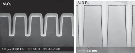
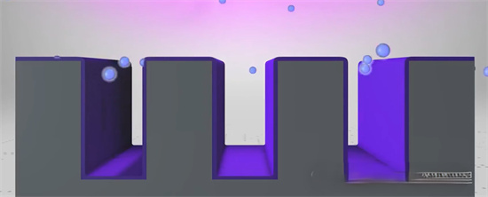
The self-limiting reaction is the core principle of ALD. In each cycle, precursor molecules can only react with active sites on the surface. Once these sites are fully occupied, subsequent precursor molecules cannot adsorb, ensuring that only one atomic or molecular layer is added per deposition cycle. This characteristic grants ALD exceptional uniformity and precision in film deposition, as illustrated in the figure below, where excellent step coverage is maintained even on complex three-dimensional structures.
III. Applications of ALD in Semiconductor Manufacturing
ALD finds extensive applications in the semiconductor industry, including but not limited to:
· High-Dielectric Constant (High-k) Material Deposition: Used for gate insulators in next-generation transistors to enhance device performance.
· Metal Gate Deposition: Such as titanium nitride (TiN) and tantalum nitride (TaN), employed to improve transistor switching speeds and efficiency.
· Interconnect Barrier Layers: Prevent metal diffusion, ensuring circuit stability and reliability.
· Three-Dimensional Structure Filling: Such as filling channels in FinFET structures to achieve higher integration densities.
Atomic Layer Deposition (ALD) has revolutionized semiconductor manufacturing with its extraordinary precision and uniformity. By mastering the ALD process flow and principles, engineers can construct high-performance electronic devices at the nanoscale, driving continuous progress in information technology. As the technology evolves, ALD will play an even more critical role in the future of the semiconductor industry.
AMTD provides high-precision Showerhead services for core components, with products primarily including Shower head, Face plate, Blocker Plate, Top Plate, Shield, Liner, pumping ring, Edge Ring, and other core semiconductor equipment parts. These products are widely used in the semiconductor and display panel industries, offering exceptional performance and high market recognition.
Content Source: WeChat Official Account: Semiconductor and Physics
上一篇:Etching Process in Semiconductor Manufacturing(Showerhead)
下一篇:Atomic Layer Deposition (ALD) and Showerhead


