


Etching is a crucial step following photolithography, where the pattern on the photoresist is precisely transferred to the underlying thin - film material. It is one of the core processes for realizing integrated circuit structures on a wafer. The quality of etching directly determines the performance and dimensions of devices, especially being vital for line - width and size control in advanced nodes. The quality of the photolithography pattern (such as resolution and line - edge roughness) forms the basis for determining the precision of the final etched pattern.
1. Classification of Etching Processes
By Etching Environment/Principle
· Dry Etching: Utilizes gaseous plasma or ion beams for etching.
o Plasma Etching: Mainly relies on chemically active free radicals.
o Ion Beam Sputter Etching: Primarily depends on physical bombardment (sputtering).
o Reactive Ion Etching (RIE): Combines chemical reactions and physical bombardment. It is currently the mainstream etching technology, capable of achieving good anisotropy.
· Wet Etching: Uses liquid chemical solutions for etching.
By Mask Requirements
· Patterned Etching: Uses photoresist or other hard masks (such as SiN or metals) to protect certain areas, and only etches the exposed parts. This is the core of pattern transfer.
· Unpatterned Etching: Etches the entire surface without a mask to protect specific areas (such as removing an entire thin - film layer or preliminary thinning before planarization).
2. Key Parameters and Issues in the Etching Process
The precision and fidelity of pattern transfer during etching rely on the control of the following key parameters:
Incomplete Etching
· Phenomenon: The material to be removed is not completely cleared.
· Causes: Insufficient etching time; uneven film thickness; lower - than - expected etching rate; poor etching uniformity; severe micro - loading effect (ARDE).
Over - Etching
· Phenomenon: The etching process continues after the target material has been completely removed.
· Purpose: To compensate for uneven film thickness, the micro - loading effect, and minor delays in etching endpoint detection, a certain degree of planned over - etching is necessary and common. However, it must be strictly controlled to avoid damaging the underlying material.
Undercutting (Drilling Etch)
· Phenomenon: Etching occurs not only downward but also laterally below the mask edge, removing the material under the mask and forming an "undercut" or "lateral recess".
· Causes: Significant isotropic etching components; poor adhesion between the mask and the underlying material (especially prominent in wet etching).
· Impact: Results in line - width loss and pattern deformation.
Selectivity
· Definition: The ratio of the etching rates of two different materials under the same etching conditions (Selectivity = Rate A / Rate B).
· Importance:
o Mask Protection: A high selectivity means that the mask material (such as photoresist) etches slowly, while the target material (such as SiO₂, Si, or metals) etches quickly. This ensures that the mask has sufficient thickness to protect the underlying layer when the target material is completely etched. Low selectivity can lead to premature depletion of the mask, damage to the pattern, or accidental etching of the underlying material.
o Stop - Layer Control: High selectivity allows the etching to precisely terminate at a specific stop - layer (such as etching SiO₂ and stopping on Si).
· Example: When using photoresist as a mask for dry etching of SiO₂, a high SiO₂: PR (photoresist) selectivity is required.
Anisotropy Degree
· Isotropic Etching: The etching rate is the same in all directions (vertical and horizontal), resulting in a rounded side - wall, easy undercutting, and poor pattern fidelity. Wet etching is usually isotropic.
· Anisotropic Etching: The etching rate in the vertical direction is much higher than that in the horizontal direction, enabling the formation of steep and clear side - walls with high pattern fidelity. Dry etching (especially RIE) can achieve a high degree of anisotropy.
Uniformity
· Definition: A parameter that measures the consistency of the etching capability (mainly rate and profile) within a single wafer, between wafers in the same batch, and between different batches of wafers.
· Importance: Non - uniformity can lead to local over - etching or incomplete etching, directly affecting device performance and yield.
· Influencing Factors and Challenges:
o Aspect - Ratio - Dependent Etching: The etching rate significantly decreases as the aspect ratio (depth/width) of the opening increases, and may even stop at high - aspect - ratio small - sized patterns. This is also known as the micro - loading effect.
o Pattern Density Effect: The etching rates in dense pattern areas and isolated pattern areas may be different.
o Equipment/Process Parameter Fluctuations: Non - uniformity in gas flow, temperature, radio - frequency power, and pressure.
Other Key Issues
· Residues and Polymers: The deposition of etching by - products on the surface or side - walls can cause short - circuits, open - circuits, or affect subsequent processes.
· Plasma - Induced Damage: The deterioration of electrical properties of sensitive structures such as gate oxides and junction regions caused by high - energy particle bombardment.
· Particle Contamination: Particles generated during the etching process fall onto the wafer surface, causing defects.
3. Comparison between Dry Etching and Wet Etching
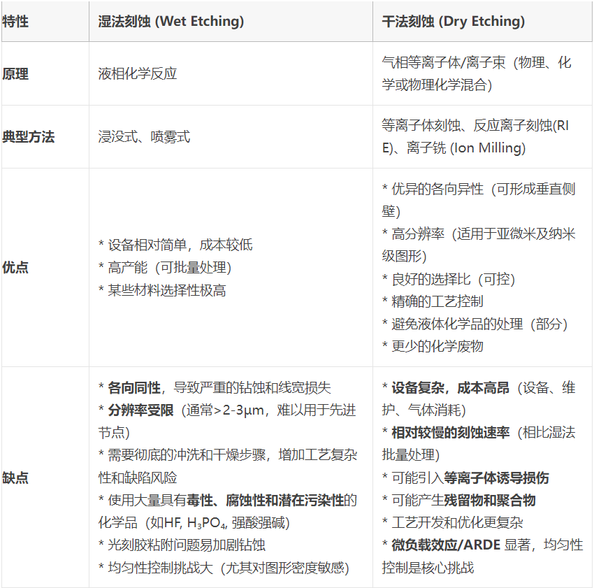
Summary
Etching is a core technology for achieving precise pattern transfer in semiconductor manufacturing. Dry etching (especially RIE and its derivative technologies) has become the absolute mainstream technology for modern advanced integrated circuit manufacturing (especially for feature sizes less than 1 µm) due to its excellent anisotropy, high resolution, good selectivity, and controllability. Although it has drawbacks such as high equipment cost and relatively slow etching rate, its advantages in pattern fidelity and size control are irreplaceable.
AMTD provides high - precision Showerhead services for core components. Its products mainly include Shower heads, Face plates, Blocker Plates, Top Plates, Shields, Liners, pumping rings, Edge Rings, and other core semiconductor equipment parts. These products are widely used in the semiconductor and display panel industries, with excellent performance and high market recognition.
Content Source: Weina Research Institute Official Account
上一篇:Analysis of the Relationship Between Dry Etching and Showerhead
下一篇:Atomic Layer Deposition (ALD) in the Semiconductor Industry


