


Overview of chemical vapor deposition
Chemical vapour deposition (CVD) refers to a thin film preparation technology that uses other forms of energy such as heat, plasma, ultraviolet irradiation, laser irradiation, etc., alone or comprehensively, to make gaseous substances undergo chemical reactions on the hot surface of solids to form stable solid substances and deposit them on the surface of wafers.
The growth process of deposition of thin films by CVD can be divided into the following steps:
(1) The gas mixture participating in the reaction is transported to the surface of the substrate;
(2) the reactant molecules diffuse from the main gas flow to the surface of the substrate;
(3) the reactant molecules are adsorbed on the substrate surface;
(4) A chemical reaction occurs between the adsorbed molecule and the gas molecule to generate silicon atoms and by-products of chemical reaction, and the silicon atoms migrate along the surface of the substrate and combine into the crystal lattice;
(5) Reaction by-product molecules are analyzed from the substrate surface;
(6) The by-product molecules diffuse from the surface of the substrate into the main gas stream, and then are discharged from the deposition area.
Chemical vapor deposition reactions must meet three volatility criteria:
(1) At the deposition temperature, the reactant must have a high enough vapor pressure to allow the reactant to be introduced into the reaction chamber at a reasonable rate. If the reactants are all gases at room temperature, the reaction apparatus can be simplified; If the volatility is very low at room temperature, the reaction agent needs to be introduced into the reaction chamber with carrying gas, in which case the gas line connected to the reactor needs to be heated to prevent the reaction from condensing.
(2) The reaction products must be volatile except for sedimentary substances.
(3) The sediment itself must have a sufficiently low vapor pressure to allow the sediment from the reaction to remain on the heated substrate.
2. The main types of chemical vapor deposition
There are six broad categories of chemical reactions used in CVD technology: pyrolysis, hydrogen reduction, composite reduction, oxidation and hydrolysis, metal reduction, and nitride and carbide generation.
Apply:
Deposition of elemental (e.g., amorphous silicon films) or simple compounds (e.g., SiO₂, pyrolysis by Si (OC₂H₅)₄), simple equipment (single-zone furnace), suitable for high-purity thin film preparation (e.g., silicon films for solar cells), but limited to thermally stable precursors.
2. Hydrogen reduction reaction
Principle:
H₂ is used as a reducing agent to reduce metal halides (e.g., chloride, fluoride) to form solid metals/semiconductors.
Typical reactions:
Apply:
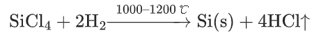
Preparation of high-purity semiconductor elemental (such as polysilicon for integrated circuits) and refractory metals (W, Mo). High temperature (>800°C), H₂ is flammable and explosive, suitable for high-temperature resistant substrates (such as silicon wafers), and is widely used for silicon epitaxial growth in chip manufacturing.
4. Oxidation reaction and hydrolysis reaction
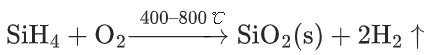
Oxidation: The precursor reacts with O2 to form oxides
Sidroli Si Kean: Teprekel Solick Tswithhar ₂ Oh (Gasfis Orliquidwater).
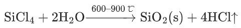
Application: Preparation of insulating oxide films (e.g. SiO₂ gate oxide layer, Al₂O₃ passivation layer). The oxidation reaction relies on high-purity O₂, and the hydrolysis reaction needs to control the partial pressure of water vapor, which is widely used in semiconductor interlayer insulation and MEMS device packaging.
5. Metal reduction reactions
Principle:
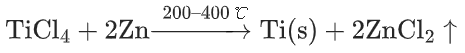
Metal halides are reduced with reactive metals (e.g., Zn, Mg) and target metals are deposited at low temperatures.
Typical reactions:
Apply:
Preparation of refractory metals (Ti, Nb) or rare metal films, suitable for plastics, ceramics and other substrates that are not resistant to high temperatures. However, the by-product metal salts need to be removed in time to avoid contamination, and are often used in the diffusion barrier layer of microelectronic devices.
6. Reaction to generate nitrides and carbides
Nitride: Precursor reacts with NH₃, N₂ (pyrolysis or reduction).
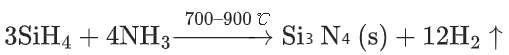
Carbide precursors react with CH₄, C₂H₂ (pyrolysis or compounding).
Applications: Nitrides (e.g. Si₃N₄ corrosion-resistant passivation layers, GaN power devices), carbides (SiC high-temperature coatings, abrasion resistant films). High temperature or plasma assistance (e.g., PECVD to reduce the temperature) is required to meet the requirements of high hardness and high thermal conductivity.
3. Activation energy of chemical vapor deposition reaction
The activation energy required for chemical vapor deposition reactions usually comes from: thermal energy, plasma, and laser.
1. Thermal activation method
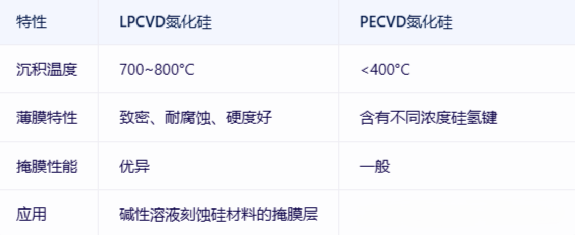
Chemical vapor deposition in the thermal energy activation method requires a certain amount of thermal energy, that is, the reaction environment needs to reach a certain temperature, and the temperature required is usually related to the pressure of the reaction gas, the smaller the pressure, the higher the temperature required. Chemical vapor deposition can be divided into atmospheric pressure chemical vapor deposition (APCVD) and low pressure chemical vapor deposition (LPCVD) according to the reaction gas pressure.
(1) Atmospheric Chemical Vapor Deposition (APCVD).
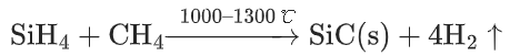
Atmospheric chemical vapor deposition was used in the semiconductor manufacturing industry to deposit oxide and silicon epitaxial layers in the early days and is still used today. Atmospheric chemical vapor deposition refers to a chemical vapor deposition method carried out under atmospheric pressure, and the reaction temperature is between 300~500 °C. The system required for this process is simple, the reaction speed is fast, and the deposition rate can exceed 10000Å/min, which is especially suitable for dielectric volume, but its disadvantages are poor uniformity, large gas consumption, and poor step coverage ability, so atmospheric pressure chemical vapor deposition is generally used in thick medium deposition.
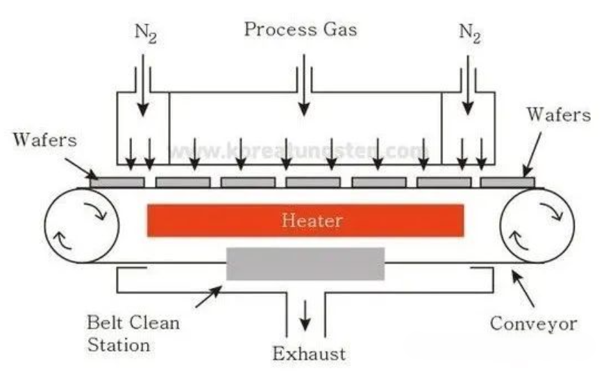
With the decrease of the characteristic size of the semiconductor process, the requirements for the uniformity of the film and the thickness error of the film continue to increase, and the low-pressure chemical vapor deposition has appeared. Low-pressure chemical vapor deposition is to reduce the pressure in the reaction chamber to 0.2~2 Torr, and the reaction temperature is between 500~900°C. Compared with atmospheric pressure chemical vapor deposition, low-pressure chemical vapor deposition thin films have good thickness uniformity, good step coverage, fast deposition rate, high production efficiency, and better performance of deposited films, so they are more widely used. Low-pressure chemical vapor deposition is often used for the deposition of polysilicon, silicon nitride films, alumina, and some metal films.
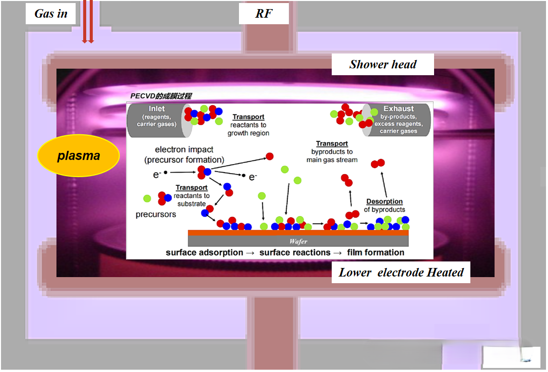
2. Prasmaaktivationmod
Chemie Calvapol de Position, Usin Pulas, Maas, Aktivatiang, Mesold, Iscalid, Prasma-Enhansed, Chemi, Calvapol, de Position (Pek). Pūsma-Enhansed, Chemi, Calvapol, Deposition, Reverstous, Ben Direct, Korente Voltaji (Dirk), Altnatin Korente Voltaji (Ake), Ladio, Frey Gunsi (Raf), Mikrovav (M), Orelek, Trensi, Klotren Resonance (Eck), Toachiv, Gas, Grody, Shege, Endlovakam, Condition, Stoprodus, Plas, Mainte de Position, Rick. Dutot, Ing, Chriss, Enajiander, Axelrat, Demovimente, Ben Posttiv, Joins, Ander, Erek, Terence, Inteplas, Maendt, Axon, Bent, Elek, Trickfield, Teschagd, Patticles, Constant, Licoli, Wes, Sinotelal Rick Tiff, Gas, Molle, Cools, Sotat, Triktiv, Gas, Ionizes, Olis, Aktivat, Into, Aktieve, Grups, Whitch, Ares, Sitto, Folm, Ander, Gretel, Retley, Edustead, Position, Temperatour.
3. Laser activation method
Chemical vapor deposition using a laser as an activation method is called laser-enhanced chemical vapor deposition. With the development of high technology, the use of laser enhanced chemical vapor deposition is also a commonly used method.
Fourth, the preparation of CVD for several films
1. SiO2 film
In this process, silicon does not participate in the reaction, but only acts as a substrate, and the oxidation temperature is very low, also known as "low temperature deposition". There are two types of silicon-containing compounds: alkoxysilanes and silanes.
(1) Alkoxysilane decomposition method
Alkoxysilane decomposition method is an organosilicide containing silicon and oxygen, usually using tetraethoxysilane, itself is liquid at room temperature, and it should be heated (40~70OC) to increase its saturated vapor pressure when used, and decompose into a SiO2 layer.
(2) Silane decomposition method
The silane decomposition method is to heat the silane in an oxygen atmosphere to react to produce silica, which is deposited on the wafer, and the oxide film produced by this method is of better quality and the growth temperature is also lower.
2. Si3N4 film
Si3N4 is a common thin film in the manufacturing process of semiconductor devices and integrated circuits, mainly used as an etching mask for SiO2. Since Si3N4 is not easily permeable by oxygen, this mask can also be used as a protective layer to prevent oxidation of the active area of the wafer surface during field oxide layer fabrication. In addition to this application, Si3N4 is also very good for alkali metal ions and is not easy to be penetrated by water and gas molecules, so it is widely used as a protective layer for semiconductor device integrated circuits. Both LPCVD and PECVD can be used to make Si3N4.
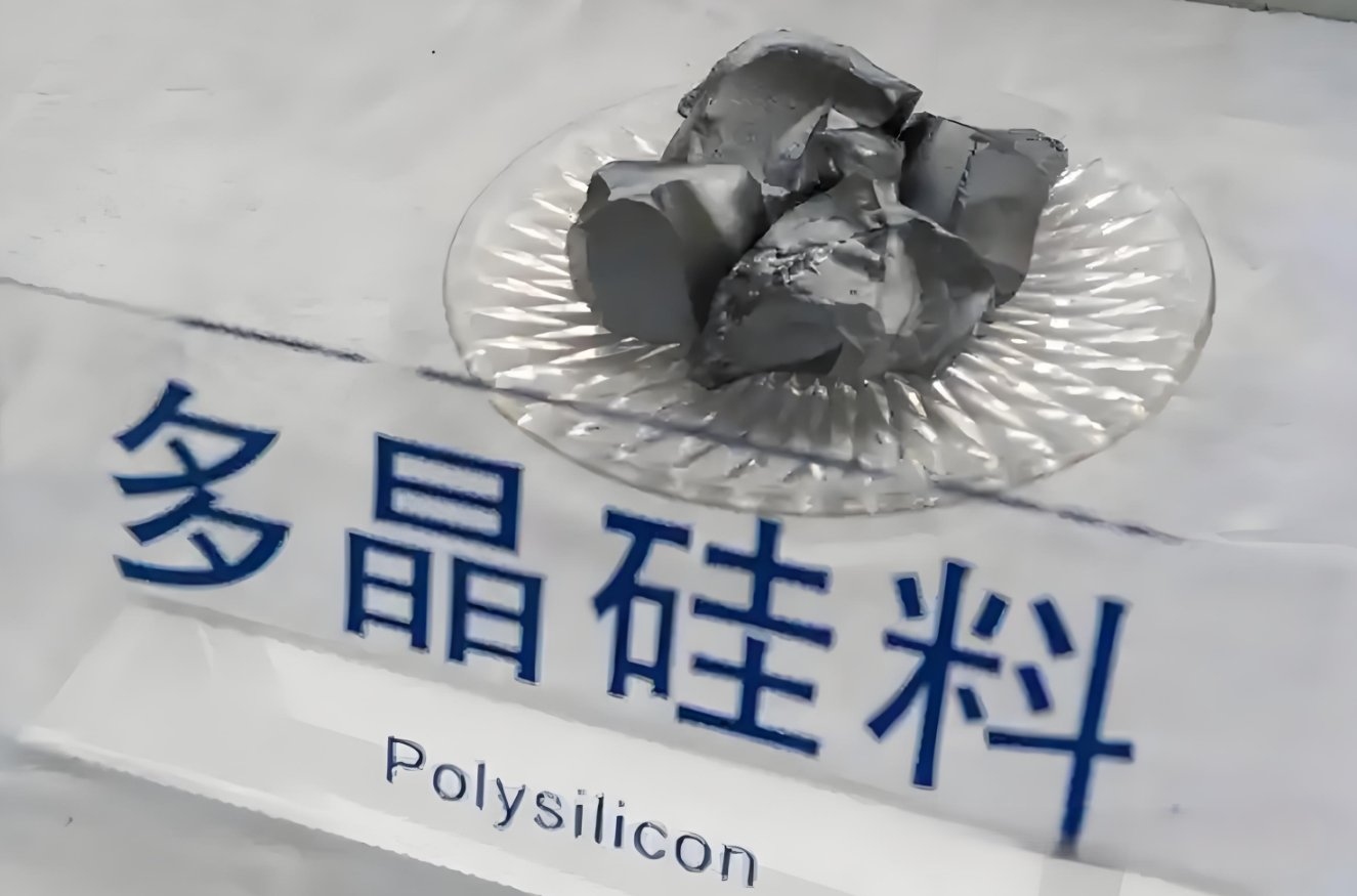
3. Polysilicon film
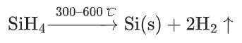
The use of polysilicon instead of metal aluminum as the gate of MOS devices is one of the major breakthroughs in MOS integrated circuit technology, which is much better than the performance of MOS devices using metal aluminum as the gate, and the use of polysilicon gate technology can realize the self-aligning ion implantation of the source and drain region, so that the integration of MOS integrated circuits has been greatly improved. Polysilicon is obtained by thermal decomposition of silane in a low-pressure reactor (600~650OC).
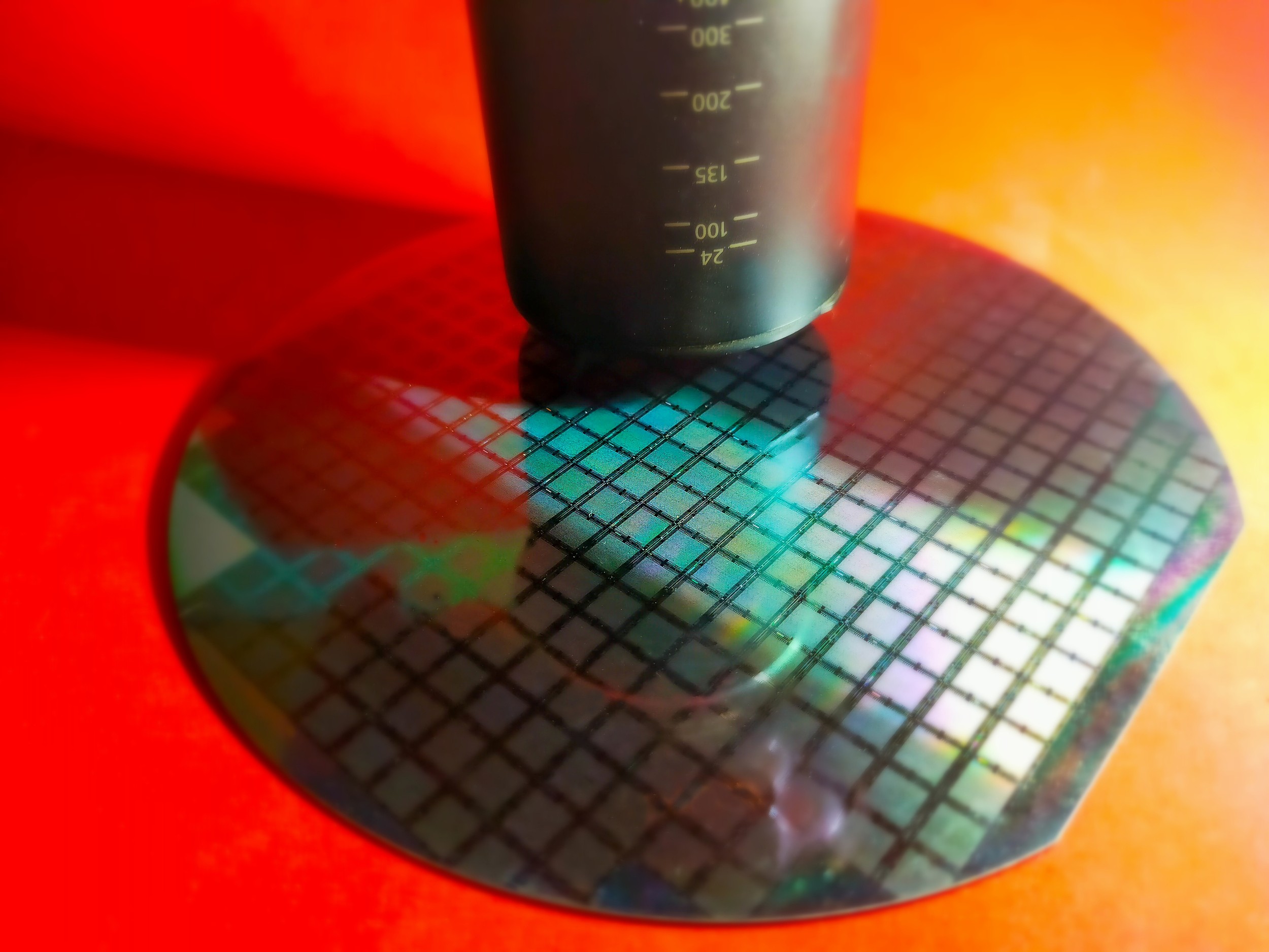
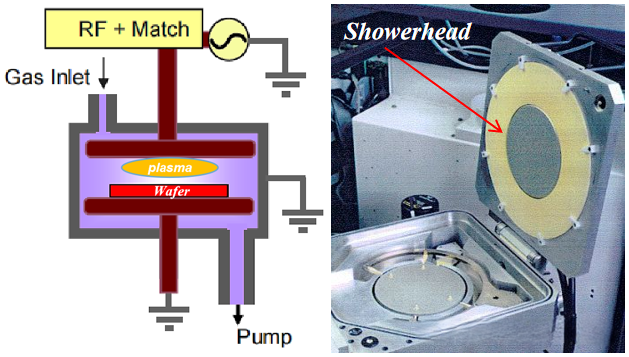
AMTD provides high-precision Showerhead services for core components, with products mainly including Showerhead, Faceplate, Blocker Plate, Top Plate, Shield, Liner, Pumping Ring, Edge Ring, and other core components of semiconductor equipment. These products are widely used in the semiconductor, display panel, and other fields, with excellent performance and high market recognition.
上一篇:Thin Film Alchemy: The Microscopic Revolution from Atoms to Chips (Part I)
下一篇:Thin-Film Alchemy: The Microscopic Revolution from Atoms to Chips (Part III)


