


Oxidation Method for Preparing Silicon Dioxide Films
When silicon is exposed to air, even at room temperature, a silicon dioxide film approximately 40 Å thick will form on its surface. This oxide layer is remarkably dense and effectively prevents further oxidation of the silicon surface by oxygen atoms. Additionally, it possesses excellent chemical stability and insulating properties. Due to these characteristics of silicon dioxide, people prepare silicon dioxide films according to various requirements, utilizing them as protective and passivation layers for devices, for electrical isolation, as insulating materials, and as dielectric films for capacitors, among other applications.
① Physical Properties of Silicon Dioxide Thin Films
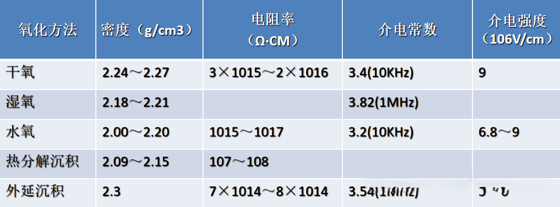
② Silicon dioxide is the most stable compound of silicon. It is insoluble in water and only reacts with hydrofluoric acid. The chemical reaction between silicon dioxide and hydrofluoric acid can be represented as follows:
SiO2 +HF → H2 [SiF6] + H2O
In industrial production, the property of silicon dioxide reacting with hydrofluoric acid is utilized to achieve the etching (corrosion) of silicon dioxide. The rate of silicon dioxide etching is influenced by factors such as the concentration and temperature of the hydrofluoric acid, the quality of the silicon dioxide, and the amount of impurities present. The etching rates can vary significantly among silicon dioxide films prepared through different methods.
Roles of Silicon Dioxide Thin Films
①As an Insulating Dielectric
Leveraging the high resistivity (~10¹⁶ Ω・cm) and stable dielectric properties (with a dielectric constant of approximately 3.9) of silicon dioxide, it is employed in semiconductor devices to isolate conductive layers (such as the gate oxide layer between the MOSFET gate and the silicon substrate). This isolation blocks leakage currents and regulates carrier behavior. Its wide bandgap (~9 eV) effectively prevents electron/hole tunneling. Additionally, as an interlayer dielectric material in integrated circuits, it prevents short-circuiting between metal interconnects, ensuring stable signal transmission and a high breakdown field strength (>10⁶ V/cm) for the devices.
②As a Masking Layer for Impurity Control
In semiconductor doping processes (such as diffusion and ion implantation), a dense silicon dioxide film (with a thickness ranging from hundreds of nanometers to micrometers), prepared through thermal oxidation or Chemical Vapor Deposition (CVD), is used to selectively block the penetration of impurities (such as boron and phosphorus) into the silicon substrate. After patterning windows through the photolithography process, doping occurs in the regions not covered by the silicon dioxide, enabling the localized fabrication of structures like PN junctions and resistors. The chemical stability and high-temperature resistance (withstanding temperatures above 1200°C) of silicon dioxide ensure that it remains uncorroded or un-decomposed during the masking process, allowing for precise control over the distribution of impurities.
③As a Surface Passivation Layer
When a silicon dioxide thin film coats the silicon surface, it can reduce the surface state density of the silicon wafer (from approximately 10¹³ cm⁻²・eV⁻¹ to below 10¹⁰), thereby suppressing carrier recombination and leakage currents caused by surface defects. Simultaneously, it acts as a barrier against environmental contaminants such as moisture, oxygen, and metal ions, preventing oxidation or corrosion of the silicon surface (for instance, avoiding sodium ion migration to the interface, which could induce threshold voltage drift). By optimizing the chemical stoichiometry at the interface (reducing dangling bonds), it also minimizes surface charge accumulation, enhancing the long-term operational stability of the device. This is particularly advantageous for power devices and sensors subjected to harsh environmental conditions, facilitating their robust encapsulation.
Preparation of Silicon Dioxide Films by Thermal Oxidation
There are numerous methods for preparing silicon dioxide, including thermal oxidation, thermal decomposition, sputtering, vacuum evaporation, anodic oxidation, plasma oxidation, and more.
1、 Three Types of Thermal Oxidation Methods
Thermal oxidation of silicon refers to the process where silicon reacts with oxygen to form silicon dioxide at high temperatures above 1000°C. The thermal oxidation method encompasses three primary approaches: dry oxidation, wet oxidation with water vapor introduction (here referred to as "water-assisted oxidation" for clarity in differentiation), and wet oxidation (using steam or a humidified oxygen environment).
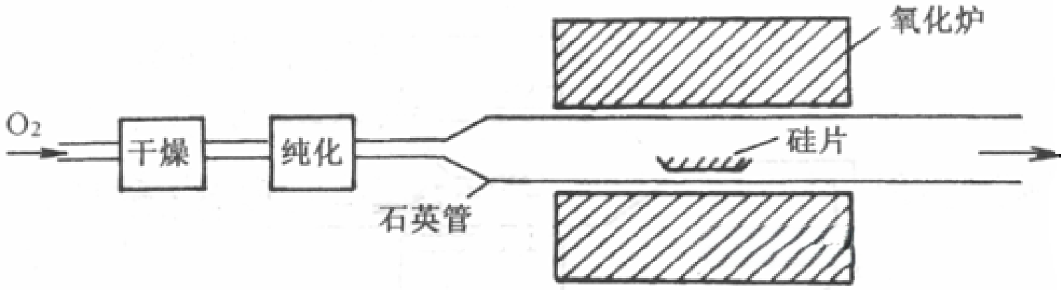
(1)Dry Oxidation
Dry oxidation involves the direct reaction of oxygen molecules with silicon at elevated temperatures to produce silicon dioxide.
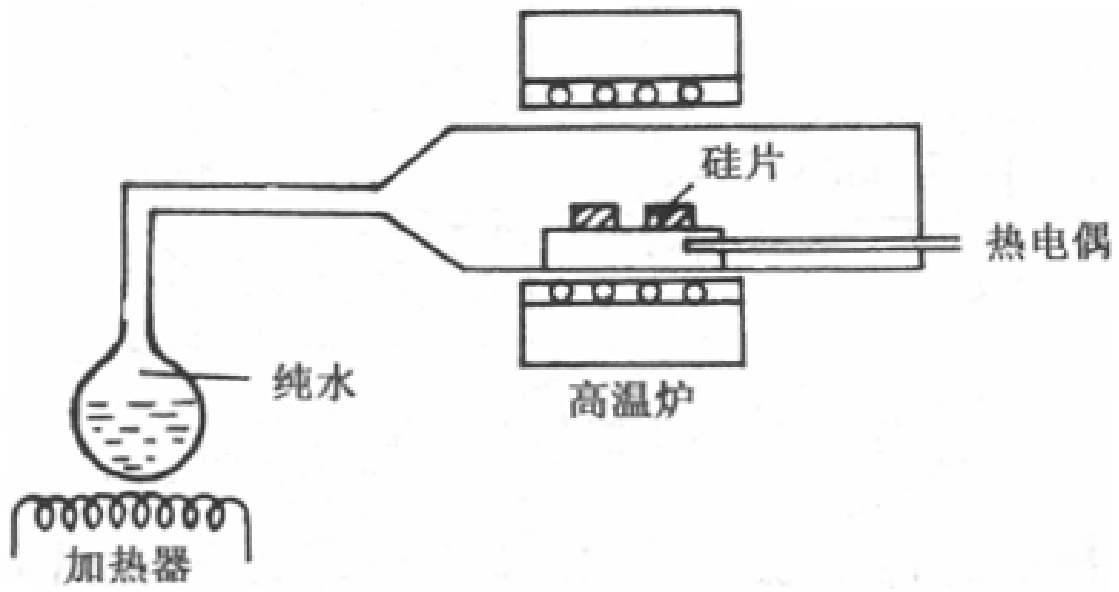
(2)Water Vapor Oxidation (Steam Oxidation)
水汽氧化是指在高温下,硅与高纯水蒸汽反应生成二氧化硅膜。Water vapor oxidation refers to the process where silicon reacts with high-purity water vapor (steam) at elevated temperatures to form a silicon dioxide film.
(3)Wet Oxidation (with Oxygen-Carrying Water Vapor)
In wet oxidation, oxygen mixed with water vapor is used instead of dry oxygen. The oxidizing agent is a mixture of oxygen and water. The reaction process is as follows: oxygen gas is passed through high-purity water maintained at 95°C, allowing it to become saturated with water vapor. This oxygen-water vapor mixture is then introduced into the oxidation furnace, where it reacts with silicon at high temperatures.
Wet oxidation can be considered a combination of dry oxidation and water vapor oxidation, with its oxidation rate falling between the two. The specific oxidation rate depends on the oxygen flow rate and water vapor content. Higher water temperatures increase the water vapor content, making the oxidation rate and film quality closer to those of pure water vapor oxidation. Conversely, lower water vapor content makes the process more akin to dry oxidation.
2、Factors Influencing Oxide Growth
① Temperature
Temperature affects the growth rate and film quality by modulating oxidation reaction kinetics and atomic diffusion. High temperatures accelerate the reaction between silicon and oxygen, increasing the diffusion coefficient and leading to exponential growth in film thickness. This promotes densification but may introduce thermal stress and impurity redistribution. Low temperatures tend to result in porous layers. Strict temperature control is required to balance performance.
② Time
The thickness of the oxide layer follows a "linear-parabolic" growth law: initially dominated by interface reactions (linear growth), followed by diffusion-controlled growth (parabolic growth, expressed as d2=Kt+C). Excessively long oxidation times can lead to excessive thickness, edge defects, or impurity accumulation. Insufficient oxidation time may result in uneven thickness or pinholes. Precise matching with process stage requirements is essential.
③ Crystal Lattice Orientation
The crystal orientation of the silicon substrate (e.g., <100>, <111>) influences the oxidation rate due to differences in atomic packing density. The <111> crystal plane, with its denser atomic arrangement, oxidizes 20%–30% slower than the <100> plane. It also exhibits lower interface state density and higher breakdown field strength. Device fabrication requires optimizing parameters according to crystal orientation to avoid thickness non-uniformity and interface defects.
④ Pressure
In gas-phase oxidation, high pressure (1–20 atm) increases the oxygen partial pressure, accelerating reactions and diffusion, making it suitable for rapidly preparing thick oxide layers but potentially introducing hydroxyl-related defects. Low pressure (<100 Pa) promotes uniform gas diffusion, improving film uniformity. However, slower growth rates necessitate elevated temperatures to compensate, balancing thickness and consistency.
⑤ Impurity Concentration
Substrate doping (e.g., n-type silicon oxidizes faster than p-type, and high boron concentration inhibits oxidation) and environmental contaminants (e.g., Na⁺ ions causing threshold voltage drift, metal ions introducing defect states) significantly influence oxidation behavior. Non-uniform doping leads to localized variations in oxidation rates, while contaminants compromise insulation performance. Strict control of silicon wafer purity and environmental cleanliness is therefore essential.
Quality Inspection of Silicon Dioxide Films
The quality of silicon dioxide films directly impacts the performance of semiconductor chips and must meet predetermined specifications. Key quality requirements include:
1、Measurement of Silicon Dioxide Film Thickness
① Colorimetric Method (Interferometric Color Estimation)
Silicon dioxide films of varying thicknesses exhibit distinct colors under illumination due to optical interference. By correlating the observed color with the interference pattern (which depends on film thickness), the film thickness can be estimated. However, this method suffers from significant measurement errors. Additionally, color differentiation becomes indistinct when the film thickness exceeds 7500 Å (750 nm), limiting its applicability to oxide films within the 1000–7000 Å (100–700 nm) range.
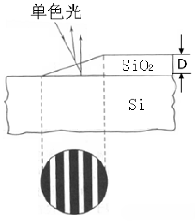
② Optical Interferometry (Wedge Etching Method)
The optical interferometry method requires etching the oxide film to form a wedge-shaped slope, as illustrated in Figure 5-3. A short-wavelength monochromatic light beam is directed perpendicularly onto the etched slope, and interference fringes are observed under a microscope at the slope. The number of interference fringes is then used to calculate the film thickness.
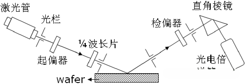
③ Ellipsometry
Ellipsometry involves illuminating the sample with elliptically polarized light and analyzing changes in the polarization state of the reflected light to determine the thickness of the film deposited on the sample.
2、Major Defects in Silicon Dioxide Films
①Non-Uniform Film Thickness
Fluctuations in deposition process parameters (e.g., temperature, pressure, gas flow rates in CVD/PVD), substrate surface roughness, inadequate pre-deposition cleaning, or uneven gas/electric field distribution in the equipment can lead to inconsistent deposition rates of silicon dioxide across the substrate surface. This results in localized regions of excessive or insufficient film thickness, causing electrical performance non-uniformities (e.g., capacitance, dielectric strength) in semiconductor devices. It also affects the uniformity of photoresist coating and subsequent etching precision, ultimately reducing chip yield and reliability.
② Surface Stains/Spots
These defects arise from particulate contaminants in the deposition environment (e.g., dust, metal ions), chemical reaction residues (incompletely decomposed precursors or byproducts), or inadequate post-deposition cleaning (residual cleaning agents). They manifest as localized protrusions or discolored areas on the film surface. Stains increase surface roughness, leading to light scattering and reduced transmittance in optical devices. In semiconductor processing, they impair photoresist adhesion, causing pattern transfer deviations (e.g., line breaks or shorts) and ultimately device malfunction.
③ Pinholes
Pinholes form due to non-uniform nucleation during deposition (e.g., atomic stacking gaps in PVD, restricted gas diffusion in CVD), substrate microdefects (e.g., pits, adsorbed impurity particles), or stress concentration-induced localized penetrating voids. Pinholes compromise film density, causing dielectric breakdown in integrated circuits and increased leakage currents or interlayer shorts. In moisture/corrosion-resistant coatings, they serve as pathways for external substances (e.g., water vapor, ions), accelerating substrate corrosion and reducing long-term device stability.
④ Sodium Ion Contamination
Sodium ions originate from deposition raw materials (e.g., gas/target materials containing sodium impurities), equipment components (e.g., sodium leaching from glass parts), or environmental exposure (e.g., residual human perspiration). They infiltrate the silicon dioxide film via ionic diffusion or electromigration. Under electric fields, sodium ions migrate to the silicon-silicon dioxide interface in semiconductor devices, altering interface charge distribution. This causes threshold voltage drift, increased leakage currents, and signal distortion in logic circuits or data errors in memory cells, potentially leading to permanent device failure.
AMTD provides high-precision Showerhead services for core components, with products mainly including Showerhead, Faceplate, Blocker Plate, Top Plate, Shield, Liner, Pumping Ring, Edge Ring, and other core components of semiconductor equipment. These products are widely used in the semiconductor, display panel, and other fields, with excellent performance and high market recognition.
上一篇:Vacuum Coating Precision: Showerhead Sprinkler Reshapes Semiconductor Film Process
下一篇:Thin Film Alchemy: The Microscopic Revolution from Atoms to Chips (Part II)


