


In the intricate chain of semiconductor manufacturing, precision machining technology serves as the critical "precision gatekeeper," ensuring that the manufacturing accuracy of components meets the required standards. The Showerhead, as a core component of the gas distribution system, has its microhole array machining accuracy directly impacting the yield and cost of chip manufacturing.
Technical Role: Full-Chain Support
The manufacturing of Showerheads encompasses various stages, including material selection, microhole machining, and surface treatment, all of which rely on precision machining technology.
Material Adaptation to Process Requirements
In high-end manufacturing processes, nickel-based alloys and titanium alloys have become commonly used materials due to their excellent performance. However, they are challenging to machine, necessitating diamond turning or honing processes to achieve micron-level surface flatness. Non-metallic materials like silicon carbide (CVD-SiC) exhibit high thermal conductivity but are prone to thermal damage during machining. Femtosecond laser cold machining technology can circumvent this issue, ensuring machining accuracy.
Overcoming the "Three Highs" in Microhole Machining
Microhole machining faces challenges related to high hardness, high density, and high precision. Traditional cutting tools are prone to wear, and stringent demands are placed on equipment positioning accuracy. In addition to femtosecond laser cold machining, advanced technologies such as electron beam machining and ion beam machining are also employed. Electron beam machining offers high precision and speed but comes with high costs and complex operation. Ion beam machining can achieve nanoscale precision and is often used for high-precision aperture machining.
Surface Treatment for Enhanced Performance
After microhole machining, surface treatment is necessary to improve performance and reliability. Chemical plating can deposit uniform coatings, enhancing corrosion and wear resistance. PVD (Physical Vapor Deposition) and CVD (Chemical Vapor Deposition) technologies can deposit functional films to improve surface properties and extend service life.
Industry Value: Yield Revolution
The improvement in precision holds significant implications for semiconductor manufacturing, directly reflected in yield enhancement and cost control.
Optimized Design for Improved Yield
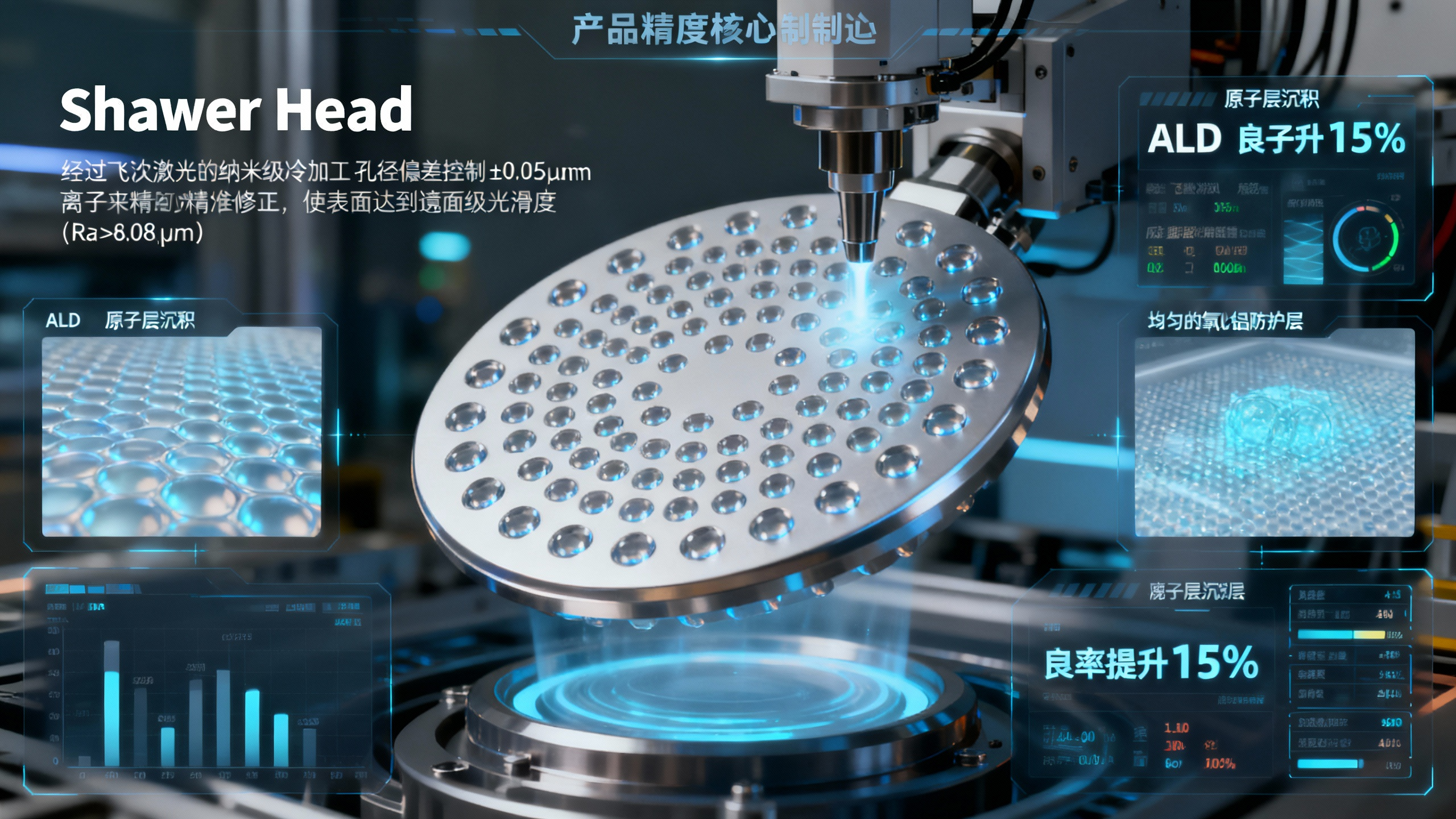
Applied Materials' ALD (Atomic Layer Deposition) Showerhead optimizes aperture distribution and flow channel design, reducing the deviation in thin-film thickness between the wafer edge and center regions from ±3% to ±0.8%. This optimization has led to a 15% increase in yield, lowering the scrap rate and production costs.
Nanoscale Correction for Advanced Upgrades
AMTD's nanoscale aperture correction technology combines femtosecond laser machining with Atomic Layer Deposition (ALD), narrowing the aperture deviation from ±0.5μm to ±0.05μm. This correction precision surpasses that of China Science Instruments, driving the yield to even higher levels and meeting the requirements of advanced manufacturing processes at 5nm and below.
Long-Term Benefits for Sustainable Development
The yield revolution brought about by precision improvement has far-reaching impacts on enterprises and the industry as a whole. High yields reduce costs and enhance efficiency for enterprises, facilitating research and development innovation and driving technological progress. Simultaneously, it improves the performance and reliability of end products, promoting the upgrading of the electronic information industry and providing support for the development of emerging fields.
Content Source: Research on Yield Improvement in Semiconductor Manufacturing, Precision Machining Technology and Applications
上一篇:Showerhead Manufacturing: The "Invisible Battlefield" of Precision Machining Technologies
下一篇:The "Revolutionary Tool" for Showerhead Microhole Machining


