


Full English Translation with Technical Context
Ion Implantation: A Physical Process for Precision Doping
Ion implantation is a critical technique for introducing controllable impurities into semiconductor substrates through a purely physical process, altering their electrical properties without chemical reactions. It is indispensable in modern silicon-based integrated circuit manufacturing, primarily used for precise doping of semiconductor materials.
Energy Loss Mechanisms (Blocking Mechanisms)
After entering the silicon substrate, ions lose energy via collisions and eventually come to rest. The energy loss mechanisms fall into two categories:
· Nuclear Blocking: Collisions between ions and lattice atomic nuclei (hard collisions) result in significant energy transfer and lattice displacement. These collisions may eject lattice atoms from their sites, causing crystal damage.
· Electronic Blocking: Interactions between ions and lattice electrons (soft collisions) involve minimal path deviation and negligible energy loss, with insignificant crystal damage.
The total blocking force (energy loss per unit distance) is expressed as:
S_total = S_n + S_e
where S_n = nuclear blocking force, S_e = electronic blocking force.
Ion Energy Range: 0.1 keV (ultra-shallow junctions) to 1 MeV (well region implantation).
· Low-energy, high-atomic-number ions: Nuclear blocking dominates.
Ion Range and Distribution
The depth at which ions stop within the substrate is called the projected range (Rp), exhibiting a statistical distribution (approximately Gaussian):
· Ions with the same energy form a depth distribution due to collision variations.
· Higher ion energy results in deeper projected ranges.
· Low-atomic-number ions (e.g., boron) have larger collision cross-sections and deeper ranges.
Process Design Implications:
1. Determines the ion energy required for specific junction depths.
2. Guides the thickness selection of implantation blocking layers.
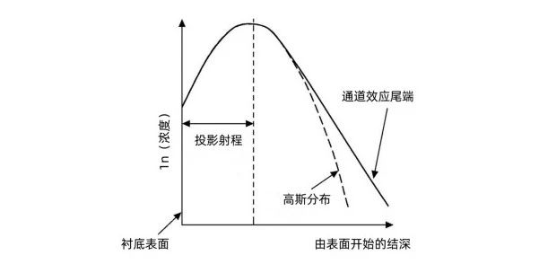
Channeling Effect
In single-crystal silicon, the regular arrangement of atoms forms crystallographic channels.
· Ions injected along these channels penetrate significantly deeper, causing undesired "tailing" in the doping profile.
· Suppression methods include tilted implantation and pre-amorphization.
· Technical Insight: Channeling is unsuitable for controlled depth doping due to its sensitivity to crystallographic orientation, leading to uniformity issues.
Technical Advantages
1. Dose Control: Precise regulation of implantation dose (10¹⁰–10¹⁷ ions/cm²) with ±2% accuracy.
2. Depth Control: Exact junction depth control via ion energy adjustment.
3. Uniformity: Scanning technology ensures in-plane doping uniformity.
4. Purity Control: Mass analyzers provide single-species ion beams.
5. Low-Temperature Process: Implantation temperatures <125°C, compatible with photoresist masks.
6. Thin-Film Penetration: Enables doping of underlying layers through surface dielectric films.
7. Beyond Solid Solubility Limit: Unconstrained by thermodynamic solid solubility limits.
Technical Limitations
1. Lattice Damage: High-energy ion bombardment induces crystal defects, requiring high-temperature annealing for repair.
2. Equipment Complexity: Involves sophisticated systems for ion source generation, acceleration, mass separation, and scanning.
AMTD specializes in manufacturing high-precision Showerhead components and other core semiconductor equipment parts, including: Showerhead, Face Plate, Blocker Plate, Top Plate, Shield, Liner, Pumping Ring, Edge Ring
Applications: Widely used in semiconductor fabrication and display panel industries, with proven performance and high market recognition.
Source: WeChat Official Account of Micro-Nano Research Institute
上一篇:The semiconductor Showerhead
下一篇:The Co-evolution of High-Precision Showerhead Manufacturing and Semiconductor Processes


