


1. Core Definition and Classification of Semiconductor Deposition Processes
Semiconductor deposition (Semiconductor Deposition) is a critical step in chip manufacturing, where thin-film materials are deposited on wafer surfaces via physical or chemical methods to form functional structures such as transistors, interconnect layers, and dielectric layers. Based on deposition mechanisms, the process is primarily classified into three categories:
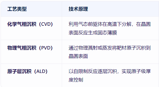
Chemical Vapor Deposition (CVD)
Physical Vapor Deposition (PVD)
Atomic Layer Deposition (ALD)
2. Key Technical Challenges and Breakthroughs in Deposition Processes
2.1 Nanoscale Film Uniformity
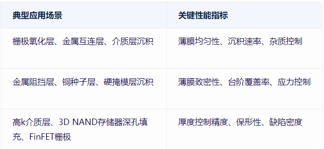
In advanced nodes (e.g., sub-3nm), gate oxide thickness must be controlled within ±0.1nm to avoid transistor threshold voltage fluctuations exceeding 5%. For example, in 3D NAND memory, ALD requires high aspect-ratio (100:1) filling with stringent conformality requirements.
2.2 Material Compatibility for Novel Materials
High-k dielectrics (e.g., HfO₂), cobalt interconnects, and 2D materials (e.g., MoS₂) are sensitive to deposition conditions, requiring process optimizations (e.g., low-temperature deposition, plasma-enhanced techniques) to address compatibility issues.
2.3 Balancing Process Efficiency and Cost
Traditional CVD has a low deposition rate (~100nm/min), while ALD is even slower (<10nm/min). Innovations like Spatial ALD, with multi-zone independent control, aim to optimize both rate and uniformity.
3. Core Equipment and Components in Deposition Processes
3.1 CVD/ALD Reaction Chambers
Chamber design directly impacts gas distribution and temperature uniformity. For example:
LPCVD reduces edge effects by minimizing gas molecule mean free path.
PECVD enhances reactivity via plasma excitation.
3.2 Showerhead (Gas Distribution Plate)
A critical component in CVD/ALD systems, the Showerhead achieves uniform gas distribution through precision-engineered aperture sizes, spacing, and flow channels. In ALD, it supports alternating precursor pulses for atomic-layer deposition.
3.3 Heating and Temperature Control Systems
The wafer chuck must maintain ±0.5℃ temperature uniformity to avoid deposition rate variations. For example, in cobalt interconnect deposition, a >1℃ temperature fluctuation may alter metal grain size and resistivity.
4. Future Trends in Deposition Processes
4.1 Advanced Packaging and Heterogeneous Integration
With 2.5D/3D packaging, deposition processes must adapt to high-density interconnects and TSV filling. For instance, ALD deposits ultra-thin barrier layers in CoWoS packaging to enhance interconnect reliability.
4.2 Intelligence and Automation
Integrated sensors and machine learning algorithms enable real-time monitoring of deposition rates, film thickness, and closed-loop process control. Applied Materials’ Endura platform supports in-line defect detection and adaptive process adjustments.
4.3 Green Manufacturing and Sustainability
Developing low-power deposition processes (e.g., low-temperature ALD), reducing precursor waste, and improving energy efficiency (e.g., from 10% in traditional CVD to 30%) are key industry priorities.
5. The "Cornerstone" Role of Deposition Processes
Semiconductor deposition is the "cornerstone" of chip manufacturing, with technological breakthroughs directly determining chip performance, power consumption, and cost. From traditional CVD to atomic-layer ALD, and from planar logic chips to 3D memory architectures, each advancement in deposition processes drives leapfrog development in the semiconductor industry.
AMTD specializes in high-precision Showerhead services for core components, including:
Showerhead, Faceplate, Blocker Plate, Top Plate, Shield, Liner, Pumping Ring, Edge Ring, and other critical semiconductor equipment parts. Applications: Semiconductor, display panel, and other industries. Advantages: Superior performance and high market recognition.
Information Sources
This content is compiled from public technical literature, equipment vendor patents, and industry conference reports. It aims to provide technical references for semiconductor practitioners. For detailed process specifics or equipment parameters, consult vendor technical white papers or contact technical teams directly.
上一篇:Showerhead: The 'Precision Heart' of Semiconductor Deposition Processes
下一篇:Common Metal Surface Treatment and Forming Processes


