


The construction differences between ICPCVD (Inductively Coupled Plasma Chemical Vapor Deposition) and CCPCVD (Capacitively Coupled Plasma Chemical Vapor Deposition) are mainly reflected in the plasma generation mechanism, core component design, and process control capabilities. The following is a detailed analysis:
I. Plasma Generation Mechanism
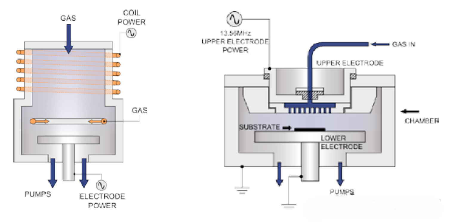
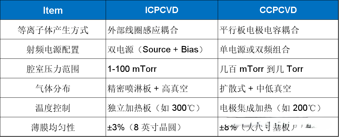
ICPCVD: It generates plasma through a high-frequency electromagnetic field induced by an external coil. The coil is typically wound around the outside of a quartz chamber. When a radio-frequency (RF) current passes through the coil, a vortex electric field is formed inside the chamber, ionizing the gas to produce high-density plasma. This method allows for independent control of plasma density (via coil power) and ion energy (via substrate bias), making it suitable for scenarios requiring high-precision film control.
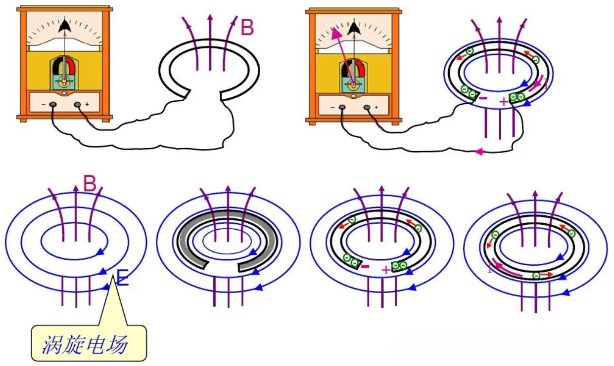
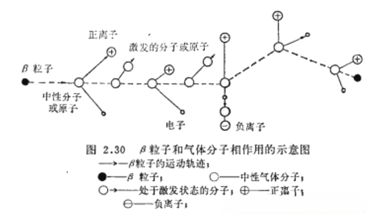
(When a gas is subjected to the action of an electric field or thermal energy, the electrons in neutral gas atoms gain sufficient energy to overcome the gravitational attraction of the atomic nucleus and become free electrons. At the same time, the neutral atoms or molecules lose the negatively charged electrons and become positively charged positive ions. This process of releasing electrons from neutral gas molecules or atoms to form positive ions is called gas ionization.)
CCPCVD: It ionizes the gas using the electric field between parallel-plate electrodes. The RF power supply is connected to the upper electrode, and the lower electrode is usually grounded and holds the substrate. The electric field directly acts on the gas molecules to generate plasma. The ion energy is directly related to the RF power and is difficult to adjust independently, making it more suitable for processes with relatively fixed ion energy requirements.
II. Core Component Design
1. Plasma Source Structure
CCPCVD
The parallel-plate electrodes are integrated into the upper and lower parts of the chamber, serving as part of the chamber itself. The structure is compact but requires regular cleaning to prevent deposition contamination.
It has a wide pressure range, typically from several hundred mTorr to several Torr, suitable for various process requirements.
ICPCVDThe coil is separated from the chamber, located outside the chamber and isolated by quartz or ceramic to avoid direct contact with the plasma and reduce the risk of contamination.
It has high vacuum compatibility, supporting lower pressures (1 - 100 mTorr), which is suitable for depositing high-quality films.
2. RF Power Configuration
CCPCVD
It uses a single power source. The RF power is directly applied to the upper electrode, and the ion energy is linearly related to the power, resulting in low adjustment flexibility.
Some advanced equipment adopts a combination of high and low frequencies (e.g., 27 MHz + 13.56 MHz) to balance plasma density and ion energy.
ICPCVD
It employs a dual-power system, usually equipped with an independent coil power source (Source RF) and a substrate bias source (Bias RF), enabling precise control of plasma density and ion energy.
The coil frequency is mostly 13.56 MHz, supporting high-power output (e.g., 1200 W).
3. Gas Distribution and Temperature Control
CCPCVD
It uses simple gas diffusion. The gas is introduced through the upper electrode or the sidewall of the chamber, and the uniformity depends on the gas flow design. Complex structures may lead to edge effects.
Temperature control is integrated with the electrode heating function, usually combined with the lower electrode. High temperature uniformity is required (e.g., ±3℃).
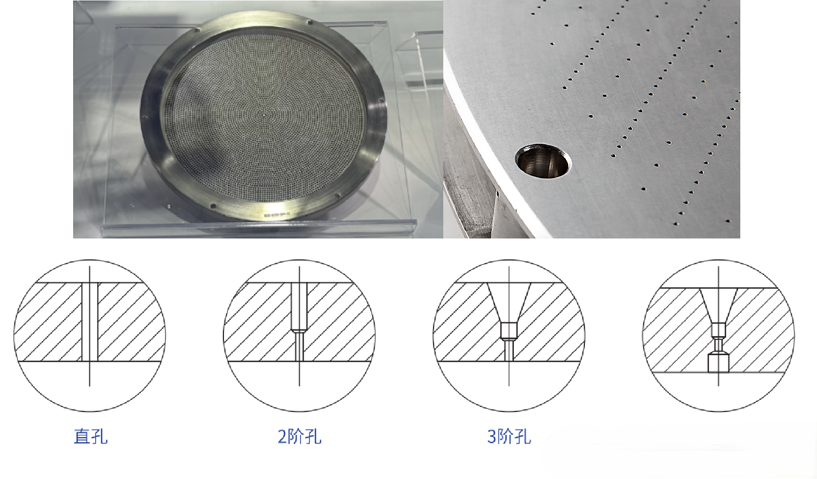
The semiconductor Showerhead is a core component of the gas distribution system in chip manufacturing. It functions similarly to a showerhead, dispersing process gases evenly into the reaction chamber to ensure the consistency, precision, and stability of critical processes such as etching and deposition.
Key Performance Indicators:
Gas uniformity: Directly affects the uniformity of film thickness and etching depth on the wafer surface (the error needs to be controlled within ±1%).
Corrosion resistance: Must withstand high temperatures, high pressures, and corrosive gases (such as CF₄ and Cl₂) in the plasma environment.
Thermal stability: Maintains structural stability during dynamic process temperature changes (200 - 600℃).
ICPCVD
It adopts a gas shower plate design. The reaction gas is introduced into the chamber through evenly distributed small holes. Combined with the high vacuum environment, it achieves film uniformity (±3%).
The substrate heating is independently controlled. The lower electrode is integrated with a heating plate (e.g., up to 300℃), supporting precise temperature gradient regulation.
III. Process Performance and Applications
CCPCVD
Advantages
Low equipment cost and simple structure, suitable for rapid deposition of materials with medium uniformity requirements, such as amorphous silicon and organic films.
Applications
Large-area coatings: PECVD is suitable for large-area and rapid deposition applications, such as solar cells and display backplanes.
Multi-layer film structures: PECVD is suitable for the preparation of multi-layer film structures, such as those used in flat-panel displays and optoelectronic devices.
Low-temperature applications: Suitable for temperature-sensitive substrates, such as organic materials and plastic substrates.
ICPCVD
Advantages
Film density: Due to the high plasma density, ICPCVD can deposit high-density, low-porosity silicon nitride films. The film density of PECVD is relatively lower.
Chemical purity: The films deposited by ICPCVD usually have higher chemical purity and lower impurity content. The films deposited by PECVD may contain more hydrogen and other impurities, but this can be improved through post-treatment.
Applications
High-performance optical coatings: Due to the high film density and low stress characteristics, ICPCVD is suitable for high-performance optical coatings, such as anti-reflection coatings and protective coatings.
Semiconductor devices: It has advantages in semiconductor devices with high precision and high reliability requirements, such as MOSFETs and MEMS devices.
High-quality insulating layers: Used for insulating layers that require high dielectric strength and low leakage current.
Summary
ICPCVD achieves independent control of plasma parameters through coil inductive coupling, making it suitable for high-precision, low-damage film deposition. In contrast, CCPCVD simplifies the structure with parallel-plate electrodes, offering lower cost but limited process flexibility. These construction differences directly determine their application divisions in semiconductor manufacturing. ICPCVD leads in key film deposition for advanced processes, while CCPCVD maintains cost-effectiveness in mid-to-low-end processes. AMTD provides high-precision Showerhead services for core components. Its products mainly include Shower heads, Face plates, Blocker Plates, Top Plates, Shields, Liners, pumping rings, Edge Rings, and other semiconductor equipment core parts. These products are widely used in fields such as semiconductors and display panels, with excellent performance and high market recognition.
Information Source: Semiconductor Army WeChat Official Account
上一篇:PECVD Process: The Value Engine in the Thin Film Deposition Segment of the Semiconductor Industry
下一篇:Showerhead: The 'Precision Heart' of Semiconductor Deposition Processes


