

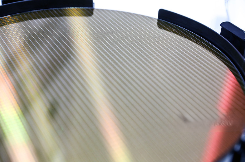


In the fields of semiconductor manufacturing and related metal processing, wafer electroplating, electroforming, and electrolysis are common yet easily confused processes. They have significant distinctions in terms of principles, application scenarios, and process parameters.
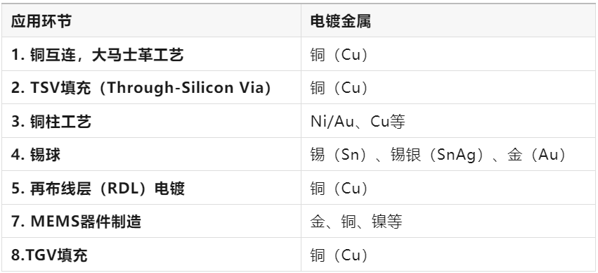
Which steps in the wafer fabrication process involve electroplating?
The table below shows the electroplating requirements for some processes.
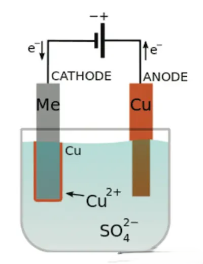
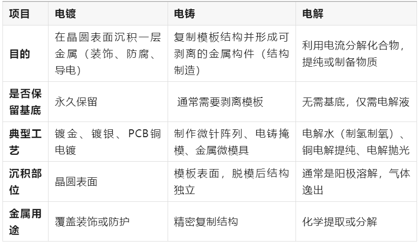
The English names of the three processes are: electroplating, electroforming, electrolysis.
In short:
In short: Electroplating: Depositing a thin metal layer onto a surface. Electroforming: Building up a thick metal deposit, then removing the mold to leave behind the formed metal structure. Electrolysis: Similar in principle to electroplating, but its primary purpose is not metal deposition on the cathode.
AMTD provides high-precision Showerhead services for core components. Its main products include Shower head, Face plate, Blocker Plate, Top Plate, Shield, Liner, pumping ring, Edge Ring, and other semiconductor equipment core parts. These products are widely used in fields such as semiconductors and display panels, with excellent performance and high market recognition.
Information source: TOM Talks About Chip Intelligent Manufacturing WeChat Official Account
上一篇:Exploring the Domestic Semiconductor Showerhead/Gas Shower Plate/Gas Distribution Plate Market
下一篇:The Evolution History of Conductor Materials: What Is the Fourth-Generation Semiconductor?


