PECVD Process: The Value Engine in the Thin Film Deposition Segment of the Semiconductor Industry
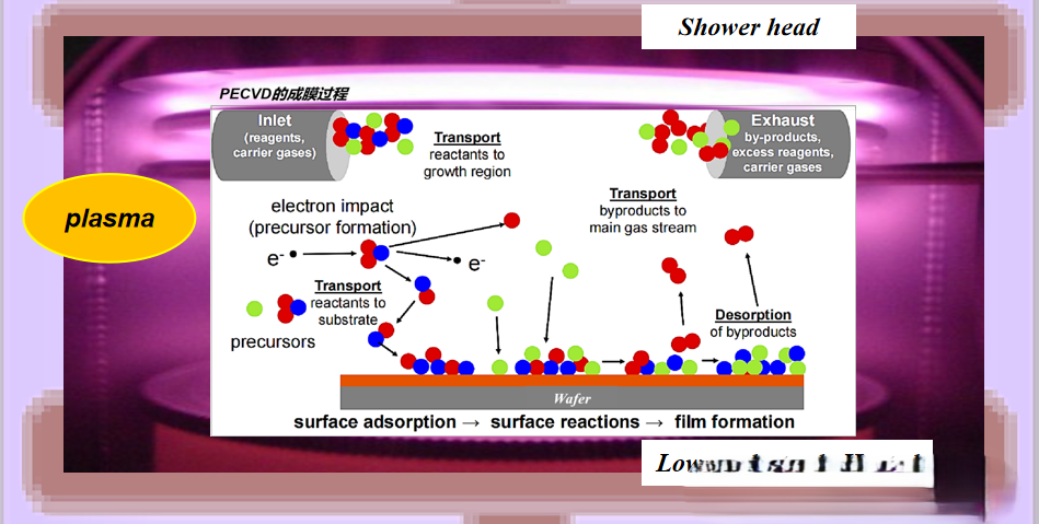
1. Introduction to the Film Formation Principle of PECVD
While traditional Chemical Vapor Deposition (CVD) technology can achieve high-precision thin films, the deposition temperatures exceeding 800°C make it unsuitable for heat-sensitive materials. How can efficient and high-quality thin film deposition be achieved at low temperatures? PECVD addresses this challenge by introducing plasma into the reaction, reducing the deposition temperature to the range of 100–400°C. Simultaneously, the use of reactive particles accelerates the reaction, increasing the deposition rate by more than tenfold.
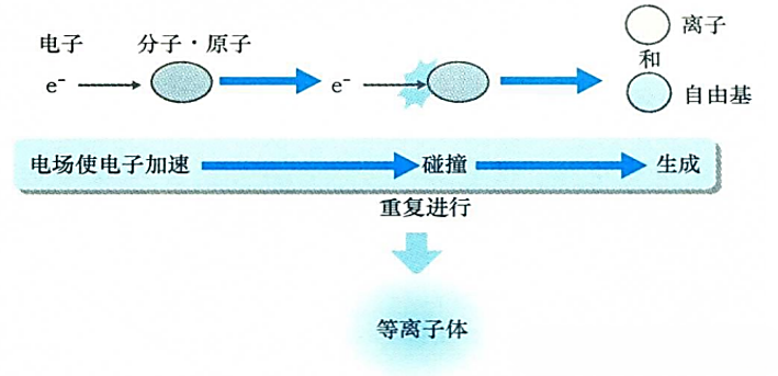
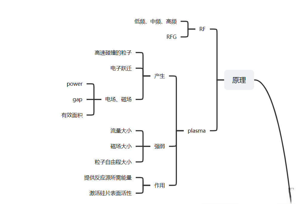
2. Plasma
In a PECVD system, an electric field is applied within the reaction chamber through radio frequency (RF) or microwave power sources, ionizing the introduced gases (such as SiH₄, NH₃, etc.) to form plasma.
Core of Film Formation:
High-energy plasma is utilized to break the chemical bonds between substances (source gases) and facilitate their recombination into new materials (such as SiNₓ, SiOₓ, SiONₓ, etc.).
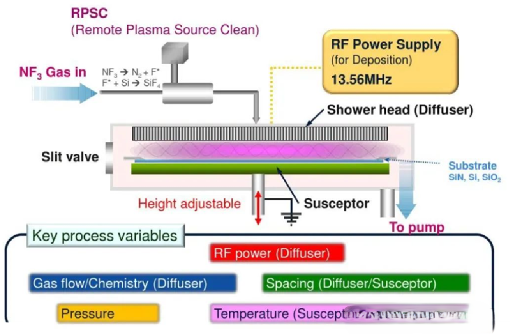
Key Controls: Gas Field and Flow Field
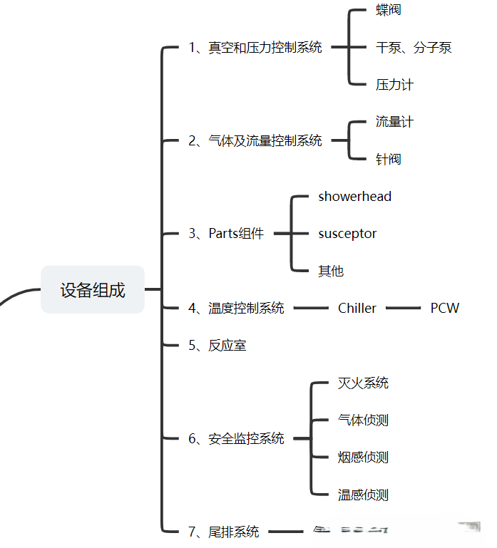
Gas Field: This refers to the control of gas pressure inside the chamber. As the pressure within the chamber changes in real-time, high-quality flow meters, pressure gauges, butterfly valves, and PID feedback control systems are crucial. Excessive pressure fluctuations can lead to product instability. Maintaining a dynamic balance between the generation and consumption of reactants during the reaction stage is essential to ensure consistency across all products. Flow Field: This pertains to the dynamic process of gas flow from the moment the source gases enter the chamber until they exit. This is why we consistently focus on the chamber environment. Insufficient cleanliness of the chamber's inner walls can lead to excessive consumption of reactive species in the flow field near the walls, thereby disrupting the deposition process. Even minor scratches or dents on the surfaces of surrounding parts can significantly impact the local flow field.
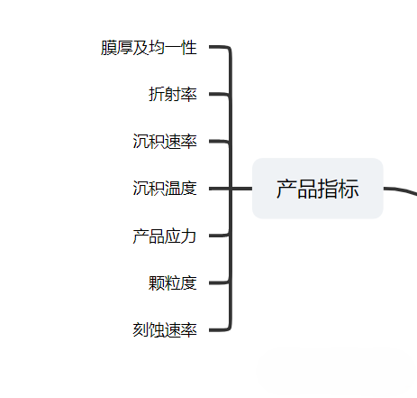
3. Process Parameters:
① Dep temp – Deposition temperature
② Thickness – Film thickness
③ Refractive Index (RI) – Refractive index
④ Stress – Film stress
⑤ Dep Rate – Deposition rate
⑥ Uniformity (WIW) – Within-wafer uniformity (the smaller the value, the better the uniformity)
⑦ Uniformity (WTW) – Wafer-to-wafer uniformity (the smaller the value, the better the uniformity)
⑧ Particle spec – Requirements for particles on the film surface
⑨ BOE Etch Rate – Buffered oxide etch rate (a parameter characterizing the film's density)
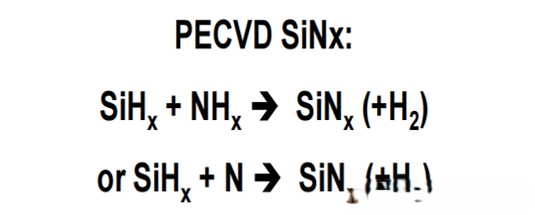
4. Gases Involved in the Reaction (Taking SiNₓ as an Example):
SiHₓ, NHₓ (typically: SiH₄, NH₃)
5. Reaction Formula:
6. Explanation of Influencing Factors:
Since the requirements for each project vary, it is necessary to conduct debugging based on one's own needs.
a. Core Principles of Debugging:
① First, fix the ratio of the compounds.
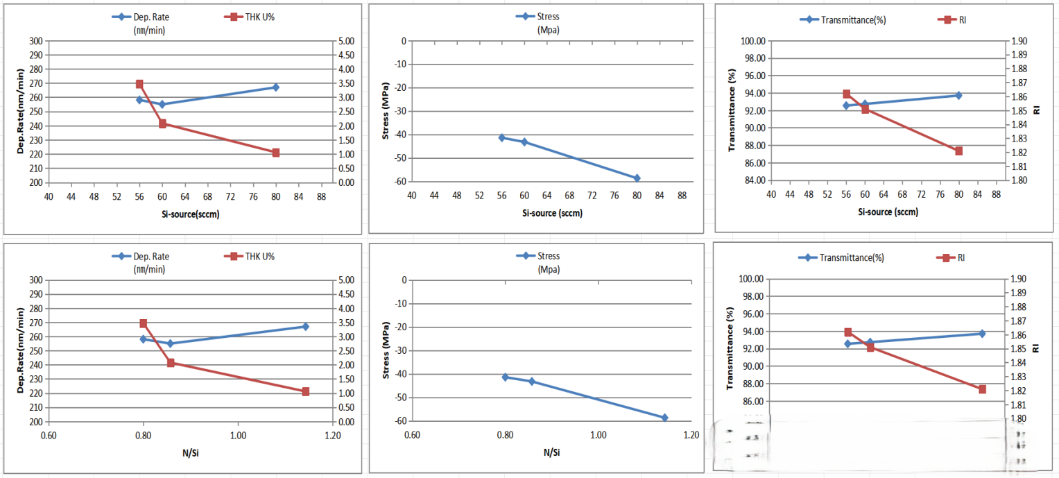
(Main impact: This has an absolute influence on the Refractive Index (RI). Debugging PECVD is challenging due to the multitude of influencing factors. When we adjust the ratio and flow rates of the compounds, the spatial gas composition within the chamber also changes. Generally, when the target values are very close to the specifications, the N/Si ratio should be kept constant. Subsequently, fine-tuning can be carried out based on your test data.)
② Process parameters (such as Pressure, Temperature, Gas flow, Gas Rate, Time, Power, etc.) exhibit linear behavior within a certain range.
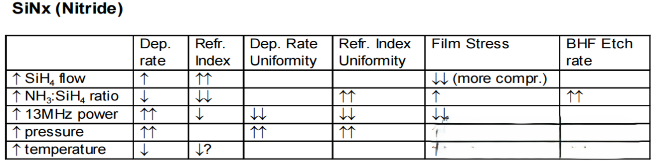
(For example, under certain conditions, as the temperature increases, the activation energy of the gases rises, intensifying the reaction and thus accelerating the deposition rate. It's important to note that I'm referring to a specific temperature range here. When the temperature becomes excessively high, the activation energy of the gases reaches saturation, and the deposition rate will remain almost unchanged, while the uniformity may deteriorate sharply, and the refractive index (RI) could also degrade. This is the challenge of the PECVD process: when you are adjusting or optimizing one parameter or indicator, other parameters and indicators may change significantly. Therefore, a comprehensive consideration is required at this stage.)
b. Memorize This Key Point:
In SiNₓ films: An increase in the silicon (Si) component leads to a higher refractive index (RI) value, whereas an increase in the nitrogen (N) component results in a lower RI value.
c. Experience Sharing:
The best recipe always ensures that all gas flow rates are set at the mid-range values of their respective Mass Flow Controllers (MFCs).
d. Operation Caution:
In a PECVD system, if the electrode gap is too large, it becomes difficult to initiate the plasma discharge; if it's too small, the electrodes are prone to breakdown.
e. Notes Sharing:
Different processes may have varying benchmarking requirements, which are provided for reference only.
Different processes may have varying benchmarking requirements, which are provided for reference only.
AMTD provides high-precision Showerhead services for core components. Its main products include Shower head, Face plate, Blocker Plate, Top Plate, Shield, Liner, pumping ring, Edge Ring, and other semiconductor equipment core parts. These products are widely used in fields such as semiconductors and display panels, with excellent performance and high market recognition.
Source of Information: WeChat Official Account "Semiconductor Army"