The Evolution History of Conductor Materials: What Is the Fourth-Generation Semiconductor?
Semiconductor materials serve as the cornerstone of the modern electronics industry, with their performance directly determining the efficiency, power consumption, and reliability of electronic devices. From the first-generation silicon-based materials to the fourth-generation ultra-wide bandgap semiconductors, each innovation in the material system has propelled leapfrog development in information technology. This article will systematically analyze the physical characteristics, technological breakthroughs, and application scenarios of the four generations of semiconductor materials, unveiling the logical chain driving industrial upgrading behind them.
I. First-Generation Semiconductors: The Founders of the Silicon-Based Era (1950s - 1980s)
Material Characteristics
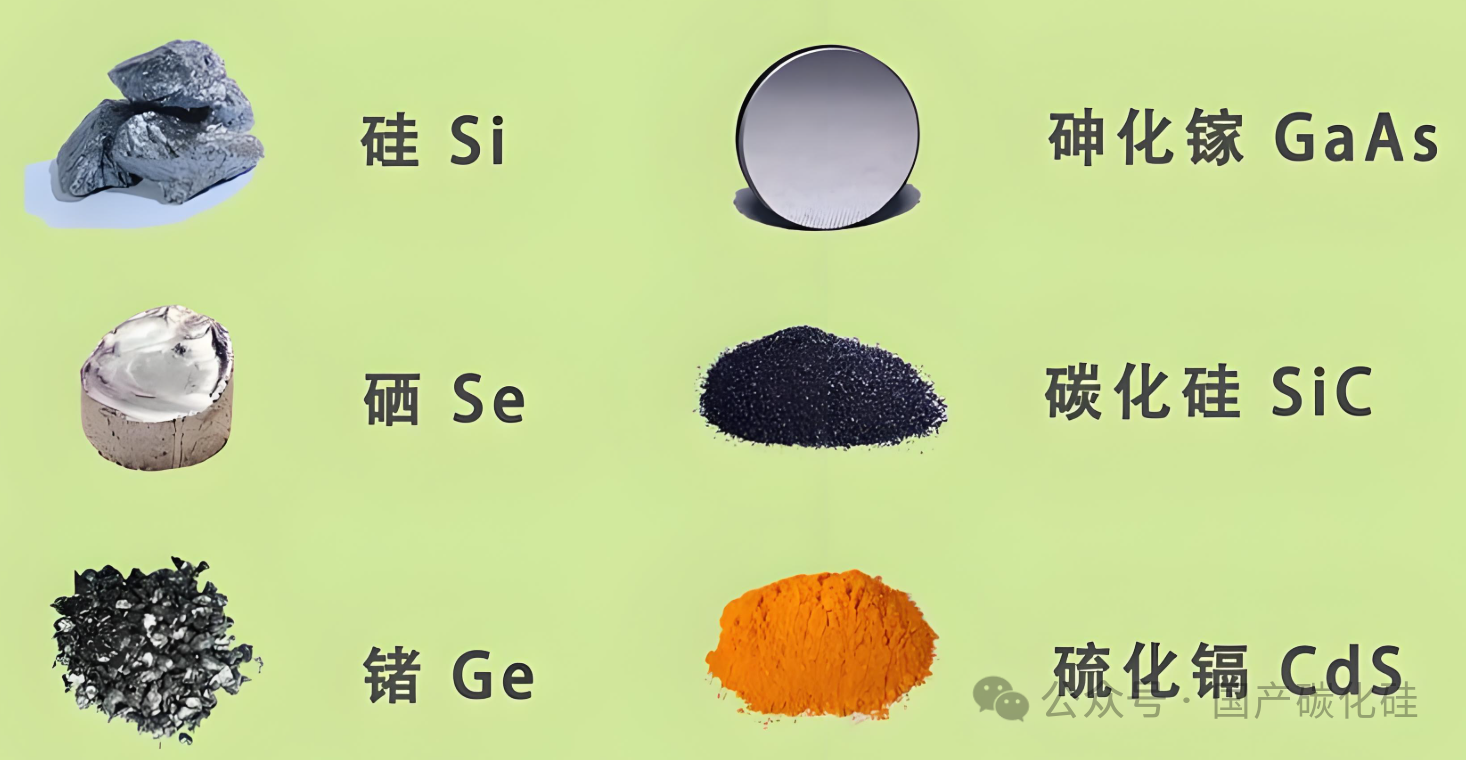
The first-generation semiconductors were centered around silicon (Si) and germanium (Ge). Silicon, with its bandgap of 1.12 eV and natural abundance (27.7% in the Earth's crust), became the absolute mainstream for integrated circuits. Although germanium had a narrower bandgap of 0.67 eV and a higher carrier mobility (3900 cm²/V·s), it was gradually replaced by silicon due to its poor thermal stability (with a maximum operating temperature of only 85°C) and scarce resources.
Technological Advantages
The success of silicon materials stems from three major breakthroughs: Silicon Dioxide (SiO₂) Passivation Technology: The SiO₂ layer generated through thermal oxidation combines excellent insulation properties and interface stability, providing the physical basis for CMOS technology. Wafer Size Upgrading: Wafer sizes have evolved from 2 inches to 18 inches (currently under development). The number of chips per wafer has increased a hundredfold, and the unit cost has dropped to $0.001 per transistor. Defect Control Technology: The dislocation density of Czochralski (CZ) monocrystalline silicon can be controlled below 10²/cm³, meeting the requirements of nanoscale processes.
Applications and Limitations
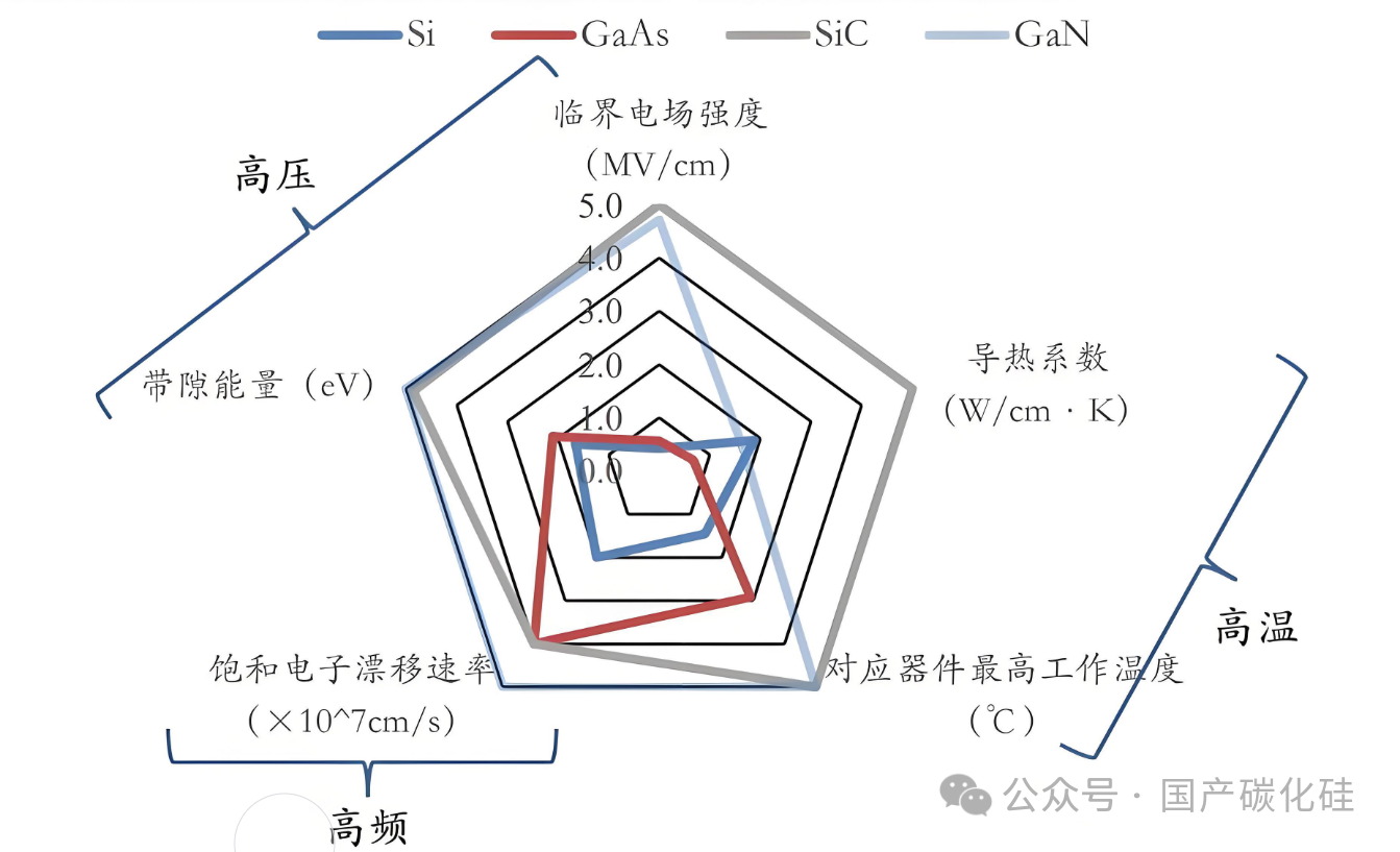
Silicon-based devices dominate over 90% of the semiconductor market, with mature processes being relied upon for CPUs, memories, and sensors. However, due to the bandgap limitation, silicon has a breakdown electric field of only 0.3 MV/cm. This results in bulky high-voltage devices (such as IGBT modules requiring multiple chips in parallel) for voltages above 600V. In scenarios like 5G millimeter-wave (frequency > 24GHz) and electric vehicle power control systems (efficiency requirements > 99%), silicon-based devices are approaching their physical limits.
II. Second-Generation Semiconductors: The Rise of Compound Semiconductors (1980s - 2010s)
Material Breakthroughs
The III-V compound semiconductors, represented by gallium arsenide (GaAs) and indium phosphide (InP), ushered in the era of high-frequency and optoelectronic applications. GaAs has an electron mobility of 8500 cm²/V·s, which is six times that of silicon, and a bandgap of 1.42 eV, enabling devices to operate at frequencies exceeding 100 GHz. InP, with its narrower bandgap of 0.76 eV, has become an ideal light-source material for the 1.55 μm optical fiber communication band.
Key Technologies Molecular Beam Epitaxy (MBE): Achieves atomic-level thickness control and enables the fabrication of high-electron-mobility transistors (HEMTs). Heterojunction Technology: The AlGaAs/GaAs heterojunction reduces the threshold current of lasers to the mA level. Semi-insulating Substrates: GaAs substrates with a resistivity of 10⁸ Ω·cm reduce radio-frequency signal losses.
Application Scenarios and Challenges
Second-generation semiconductors dominate applications such as power amplifiers in mobile communication base stations (GaAs PAs achieve 65% efficiency), VCSEL lidar (with a wavelength of 850 nm), and satellite communication systems (Q-band at 40 GHz). However, their high toxicity (arsenides), small wafer sizes (maximum 6 inches), and poor thermal conductivity (GaAs has a thermal conductivity of 0.55 W/cm·K) limit their expansion into the power electronics field.
III. Third-Generation Semiconductors: Disruptive Advances with Wide Bandgap Materials (2010s - Present)
Leap in Performance
Silicon carbide (SiC) and gallium nitride (GaN) have bandgaps of 3.2 eV and 3.4 eV, respectively, and breakdown electric fields of 3 MV/cm (10 times that of silicon). The 4H polytype of SiC combines high thermal conductivity (4.9 W/cm·K), while GaN achieves a two-dimensional electron gas (2DEG) with a sheet density of 1×10¹³ cm⁻² through the AlGaN/GaN heterojunction.
Breakthroughs in Manufacturing Technologies SiC Crystal Growth: The physical vapor transport (PVT) method enables mass production of 6-inch wafers with a micropipe density of <0.5 cm⁻². GaN-on-Si Epitaxy: Heteroepitaxy on 8-inch silicon substrates reduces costs by 80% compared to SiC. Vertical Structure Devices: For example, SiC MOSFETs achieve an on-resistance as low as 2 mΩ·cm² and reduce switching losses by 70%.
Industrial Applications
New Energy Vehicles: Tesla's Model 3 adopts SiC MOSFETs, improving the efficiency of the electric drive system by 5% and increasing range by 10%. Fast Charging Technology: GaN HEMT devices reduce the size of 65W chargers by 50% and achieve an efficiency of >92%.5G Base Stations: GaN RF power amplifiers deliver an output power of 64W (28 GHz) and are 15% more efficient than LDMOS.
IV. Fourth-Generation Semiconductors: Synergy of Ultra-Wide and Ultra-Narrow Bandgap Materials (2020s - Future)
Divergence in Material Systems
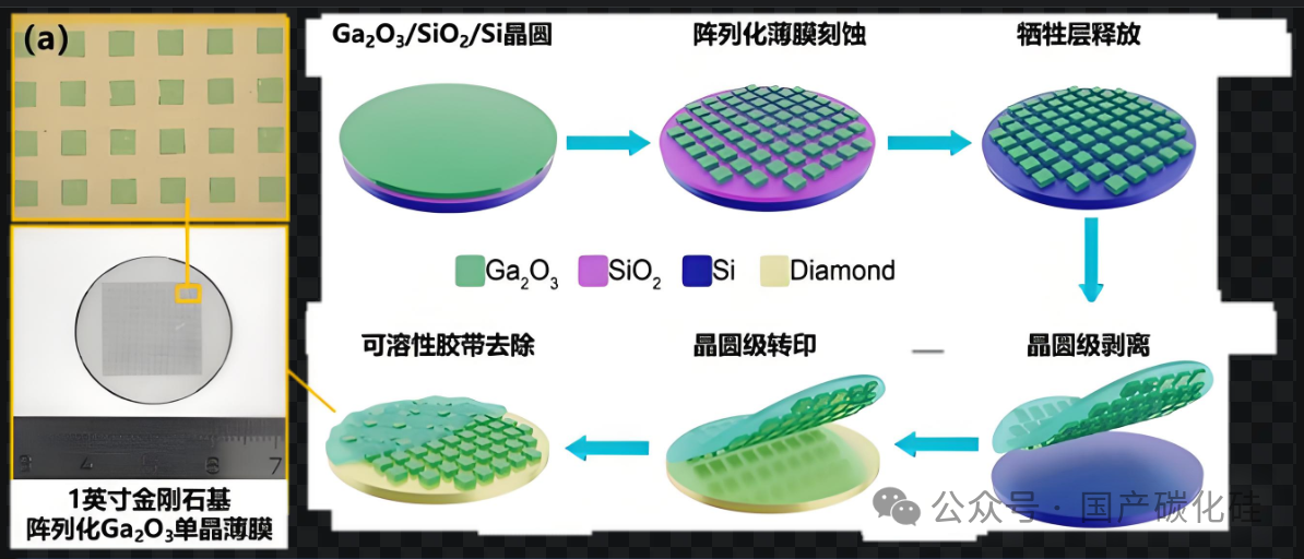
The fourth-generation semiconductors are developing in two directions: "ultra-wide" and "ultra-narrow" bandgap materials. Ultra-Wide Bandgap Materials: Gallium oxide (Ga₂O₃, 4.8 eV) and diamond (5.47 eV) have breakdown field strengths of >8 MV/cm and are suitable for ultra-high-voltage devices above 10 kV. Ultra-Narrow Bandgap Materials: Gallium antimonide (GaSb, 0.73 eV) and indium antimonide (InSb, 0.17 eV) are used for detectors in the mid-infrared to terahertz bands.
Key Technological Advances Melt Growth of Gallium Oxide: Japan's NCT Corporation has mass-produced 4-inch β-Ga₂O₃ wafers at a cost that is only 1/5 of SiC. Bandgap Engineering: InAs/GaSb type-II superlattices achieve a quantum efficiency of >80% for infrared detection in the 3-5 μm range.
Application Prospects and Challenges
Power Electronics: Ga₂O₃ Schottky diodes theoretically withstand voltages up to 8 kV and have an on-resistance of 0.1 mΩ·cm², but their low thermal conductivity (0.25 W/cm·K) necessitates bonding with diamond substrates for heat dissipation. Deep Ultraviolet Optoelectronic Devices: AlN LEDs with wavelengths as low as 210 nm can be used for water sterilization and biochemical detection, but their external quantum efficiency is less than 5%. Quantum Computing: Diamond nitrogen-vacancy (NV) color centers can achieve quantum bit coherence times of >1 ms at room temperature.
AMTD provides high-precision Showerhead services for core components. Its main products include Shower head, Face plate, Blocker Plate, Top Plate, Shield, Liner, pumping ring, Edge Ring, and other semiconductor equipment core parts. These products are widely used in fields such as semiconductors and display panels, with excellent performance and high market recognition.
Disclaimer: All information is sourced from publicly available channels on the internet. The purpose of republishing this content is to disseminate more information and does not imply that this official account endorses the views expressed or takes responsibility for their authenticity.